 |
|
| • Patented integrated digital temperature compensation
circuitry allows for near closed loop accuracy over
temperature in an open loop sensor |
• UL60950-1 (ed. 2) certified
□ Dielectric Strength Voltage = 2.4 kVrms
□ Basic Isolation Working Voltage = 420 Vpk/297
Vrms |
| • Industry-leading noise performance with greatly
improved bandwidth through proprietary amplifier and
filter design techniques |
| • Pin-selectable band width: 80 kHz for high bandwidth
applications or 20 kHz for low noise performance |
| • 0.65 mΩ primary conductor resistance for low power
loss and high inrush current withstand capability |
| • Small footprint, low-profile SOIC8 package suitable for
space-constrained applications |
| • Integrated shield virtually eliminates capacitive coupling
from current conductor to die, greatly suppressing output
noise due to high dv/dt transients |
| • 3 to 3.6 V, single supply operation |
|
| CATALOG |
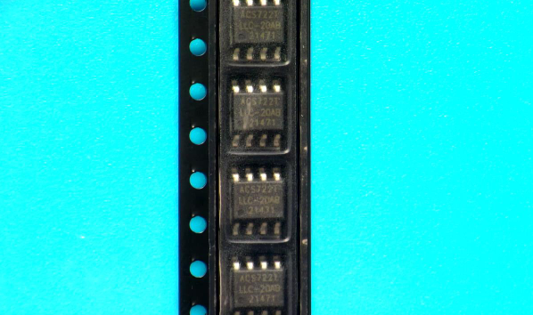
| ACS722LLCTR-20AB-T COUNTRY OF ORIGIN |
| ACS722LLCTR-20AB-T PARAMETRIC INFO |
| ACS722LLCTR-20AB-T PACKAGE INFO |
| ACS722LLCTR-20AB-T MANUFACTURING INFO |
| ACS722LLCTR-20AB-T PACKAGING INFO |
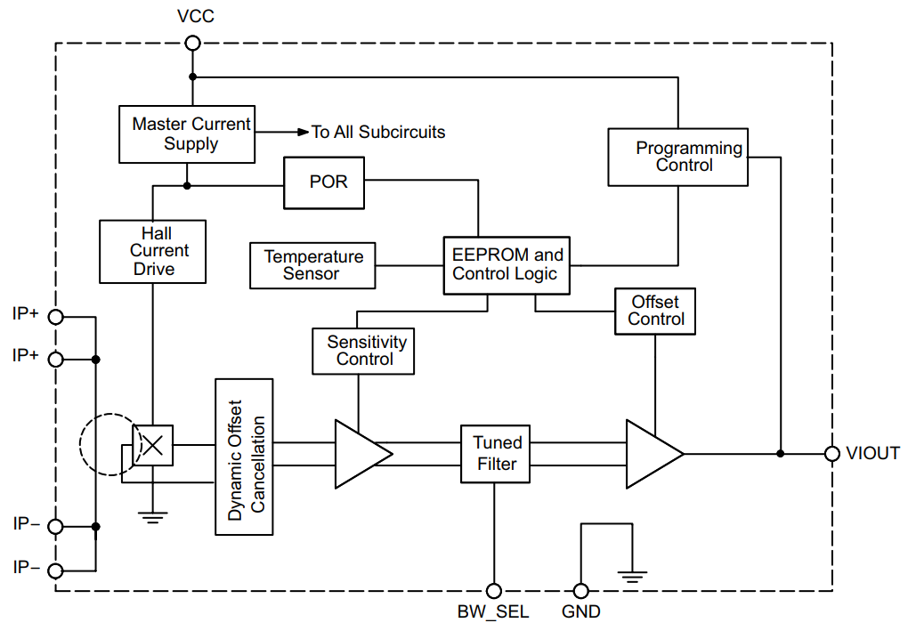
| ACS722LLCTR-20AB-T FUNCTIONAL BLOCK DIAGRAM
|
|
| COUNTRY OF ORIGIN |
| Philippines |
|
| PARAMETRIC INFO |
| Type |
Open Loop |
| Sensing Current Type |
AC|DC |
| Accuracy (%) |
±3 |
| Typical Response Time (us) |
22.5 |
| Sensitivity (mV/A) |
66 |
| Operating Frequency (kHz) |
80 |
| Maximum Output Voltage (V) |
25 |
| Maximum Isolation Voltage |
2400Vrms |
| Primary Current Measuring Range (A) |
±20 |
| Measuring Principle |
Hall Effect |
| Minimum Operating Supply Voltage (V) |
3 |
| Process Technology |
BiCMOS |
| Typical Operating Supply Voltage (V) |
3.3 |
| Maximum Operating Supply Voltage (V) |
3.6 |
| Minimum Operating Temperature (°C) |
-40 |
| Maximum Operating Temperature (°C) |
150 |
| Module/IC Classification |
IC |
| Maximum Storage Temperature (°C) |
165 |
| Minimum Storage Temperature (°C) |
-65 |
|
|
| PACKAGE INFO |
| Supplier Package |
SOIC N |
| Basic Package Type |
Lead-Frame SMT |
| Pin Count |
8 |
| Lead Shape |
Gull-wing |
| PCB |
8 |
| Tab |
N/R |
| Pin Pitch (mm) |
1.27 |
| Package Length (mm) |
4.9 |
| Package Width (mm) |
3.9 |
| Package Height (mm) |
1.5(Max) |
| Package Diameter (mm) |
N/R |
| Seated Plane Height (mm) |
1.75(Max) |
| Mounting |
Surface Mount |
| Package Material |
Plastic |
| Package Description |
Small Outline IC Narrow Body |
| Package Family Name |
SO |
| Jedec |
MS-012AA |
| Package Outline |
Link to Datasheet |
|
|
| MANUFACTURING INFO |
| MSL |
2 |
| Maximum Reflow Temperature (°C) |
260 |
| Reflow Solder Time (Sec) |
20 to 40 |
| Number of Reflow Cycle |
3 |
| Standard |
J-STD-020C |
| Reflow Temp. Source |
Link to Datasheet |
| Maximum Wave Temperature (°C) |
N/R |
| Wave Solder Time (Sec) |
N/R |
| Wave Temp. Source |
Link to Datasheet |
| Lead Finish(Plating) |
Matte Sn annealed |
| Under Plating Material |
N/A |
| Terminal Base Material |
Cu Alloy |
|
|
| PACKAGING INFO |
| Packaging |
Tape and Reel |
| Quantity Of Packaging |
3000 |
|
|
| FUNCTIONAL BLOCK DIAGRAM
|
 |
| |
|