 |
|
| • Industry-leading noise performance through proprietary
amplifier and filter design techniques |
| • Integrated shield greatly reduces capacitive coupling
from current conductor to die due to high dV/dt signals,
and prevents offset drift in high-side, high-voltage
applications |
| • Total output error improvement through gain and offset
trim over temperature |
| • Small package size, with easy mounting capability |
| • Monolithic Hall IC for high reliability |
| • Ultralow power loss:100 µΩ internal conductor
resistance |
| • Galvanic isolation allows use in economical, high-side
current sensing in high-voltage systems |
| • AEC-Q100 qualified |
| • 3.0 to 5.5 V, single supply operation |
| • 120 kHz typical bandwidth |
| • 3 µs output rise time in response to step input current |
| • Output voltage proportional to AC or DC currents |
| • Factory-trimmed for accuracy |
| • Factory-trimmed for accuracy |
| • Nearly zero magnetic hysteresis |
|
| CATALOG |
| ACS758LCB-050B-PFF-T COUNTRY OF ORIGIN |
| ACS758LCB-050B-PFF-T PARAMETRIC INFO |
| ACS758LCB-050B-PFF-T PACKAGE INFO |
| ACS758LCB-050B-PFF-T MANUFACTURING INFO |
| ACS758LCB-050B-PFF-T PACKAGING INFO |
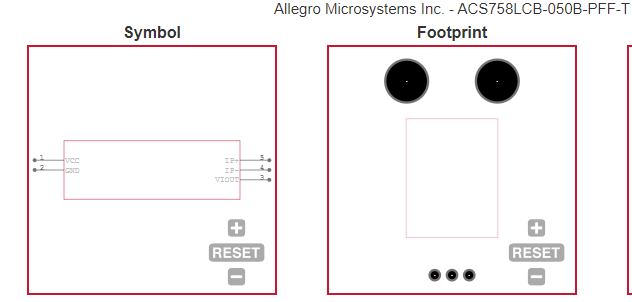
| ACS758LCB-050B-PFF-T ECAD MODELS |
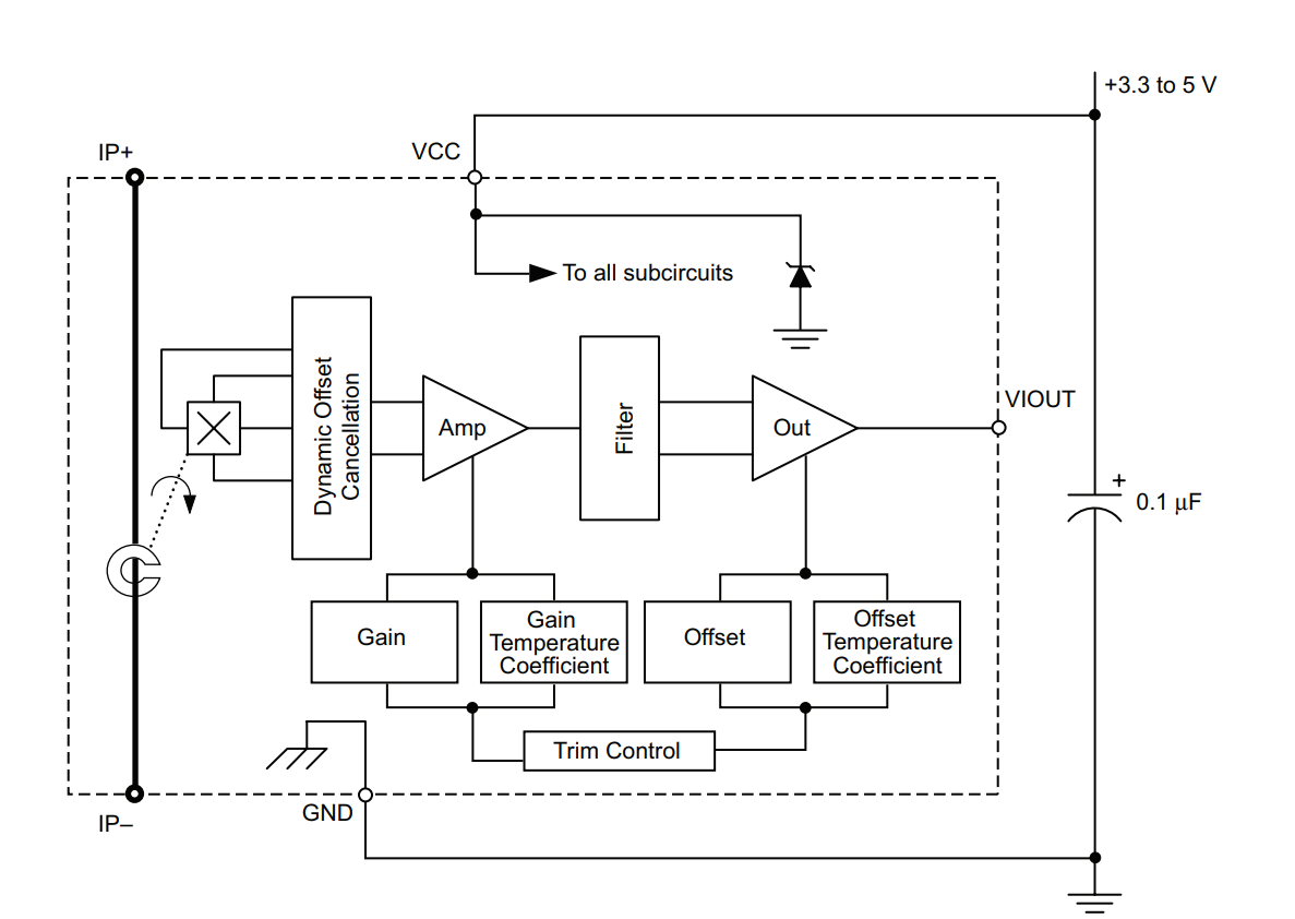
| ACS758LCB-050B-PFF-T FUNCTIONAL BLOCK DIAGRAM |
|
| COUNTRY OF ORIGIN |
| Philippines |
| Taiwan (Province of China) |
|
| PARAMETRIC INFO |
| Type |
Open Loop |
| Typical RMS Primary Current (A) |
±50 |
| Sensing Current Type |
AC|DC |
| Accuracy (%) |
2 |
| Typical Response Time (us) |
4 |
| Sensitivity (mV/A) |
40 |
| Operating Frequency (kHz) |
120 |
| Maximum Output Voltage (V) |
28 |
| Minimum Operating Supply Voltage (V) |
3 |
| Typical Operating Supply Voltage (V) |
5 |
| Maximum Operating Supply Voltage (V) |
5.5 |
| Minimum Operating Temperature (°C) |
-40 |
| Maximum Operating Temperature (°C) |
150 |
| Module/IC Classification |
IC |
| Supplier Temperature Grade |
Automotive |
| Maximum Storage Temperature (°C) |
150 |
| Minimum Storage Temperature (°C) |
-65 |
|
| |
| PACKAGE INFO |
| Supplier Package |
Case CB-PFF |
| Basic Package Type |
Through Hole |
| Pin Count |
5 |
| Lead Shape |
Through Hole |
| PCB |
5 |
| Tab |
N/R |
| Pin Pitch (mm) |
1.9 |
| Package Length (mm) |
10 |
| Package Width (mm) |
13 |
| Package Height (mm) |
7 |
| Package Diameter (mm) |
N/R |
| Seated Plane Height (mm) |
N/A |
| Mounting |
Through Hole |
| Package Material |
Plastic |
| Package Description |
N/A |
| Package Family Name |
Case CB-PFF |
| Jedec |
N/A |
|
| |
| MANUFACTURING INFO |
| MSL |
N/R |
| Maximum Reflow Temperature (°C) |
N/R |
| Reflow Solder Time (Sec) |
N/R |
| Maximum Wave Temperature (°C) |
245 to 270 |
| Wave Solder Time (Sec) |
10 |
| Wave Temp. Source |
Link to Datasheet |
| Lead Finish(Plating) |
Matte Sn annealed |
| Under Plating Material |
N/A |
| Terminal Base Material |
Cu Alloy |
|
| |
| PACKAGING INFO |
|
|
| |
| ECAD MODELS |
 |
|
| FUNCTIONAL BLOCK DIAGRAM |
 |
|