 |
|
| • High CMV Isolation: 2500 V rms Continuous
3500 V Peak Continuous |
| • Small Size: 1.00" 3 2.10" 3 0.350" |
| • Three-Port Isolation: Input, Output, and Power |
| • Low Nonlinearity: 60.012% max |
| • Wide Bandwidth: 20 kHz Full-Power (–3 dB) |
| • Low Gain Drift: 625 ppm/8C max |
| • High CMR: 120 dB (G = 100 V/V) |
| • Isolated Power: 615 V @ 65 mA |
| • Uncommitted Input Amplifier |
|
| CATALOG |
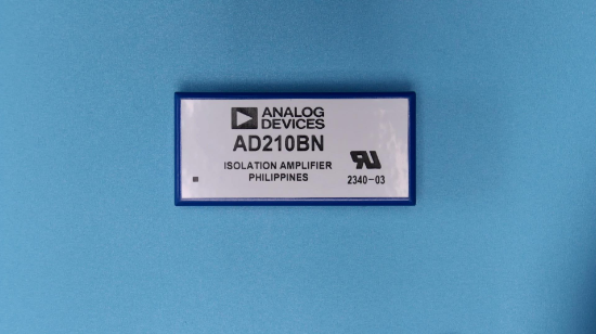
| AD210BN COUNTRY OF ORIGIN |
| AD210BN PARAMETRIC INFO |
| AD210BN PACKAGE INFO |
| AD210BN MANUFACTURING INFO |
| AD210BN PACKAGING INFO |
| AD210BN ECAD MODELS |
| AD210BN FUNCTIONAL BLOCK DIAGRAM |
| AD210BN APPLICATIONS |
|
| COUNTRY OF ORIGIN |
| Philippines |
|
| PARAMETRIC INFO |
| Type |
Isolation Amplifier |
| Number of Elements per Chip |
2 |
| Number of Channels per Chip |
3 |
| Maximum Input Bias Current (uA) |
0.00003(Typ)@15V |
| Minimum CMRR (dB) |
120(Typ) |
| Maximum Quiescent Current (mA) |
50(Typ)@15V |
| Minimum CMRR Range (dB) |
120 to 130 |
| Minimum DC Continuous Isolation Voltage (V) |
3500(Typ) |
| Maximum Input Resistance (MOhm) |
1000000(Typ)@15V |
| Maximum Voltage Gain Range (dB) |
35 to 50 |
| Maximum Voltage Gain (dB) |
40 |
| Minimum Operating Temperature (°C) |
-40 |
| Maximum Operating Temperature (°C) |
85 |
| Power Supply Type |
Single |
| Maximum Supply Voltage Range (V) |
15 to 18 |
| Minimum Single Supply Voltage (V) |
13.5 |
| Typical Single Supply Voltage (V) |
15 |
| Maximum Single Supply Voltage (V) |
16.5 |
| Maximum Operating Supply Voltage (V) |
16.5 |
| Maximum Supply Current (mA) |
80(Typ)@15V |
|
| |
| PACKAGE INFO |
| Supplier Package |
PDIP |
| Basic Package Type |
Through Hole |
| Pin Count |
12 |
| Lead Shape |
Through Hole |
| PCB |
12 |
| Tab |
N/R |
| Package Length (mm) |
53.34(Max) |
| Package Width (mm) |
25.4(Max) |
| Package Height (mm) |
8.9(Max) |
| Package Diameter (mm) |
N/R |
| Mounting |
Through Hole |
| Package Material |
Plastic |
| Package Description |
Plastic Dual In Line Package |
| Package Family Name |
DIP |
| Package Outline |
Link to Datasheet |
|
| |
| MANUFACTURING INFO |
| MSL |
N/R |
| Maximum Reflow Temperature (°C) |
N/R |
| Reflow Solder Time (Sec) |
N/R |
| Maximum Wave Temperature (°C) |
N/A |
| Wave Solder Time (Sec) |
N/A |
| Wave Temp. Source |
Link to Datasheet |
| Lead Finish(Plating) |
SnPb |
| Under Plating Material |
N/A |
| Terminal Base Material |
N/A |
|
| |
| PACKAGING INFO |
| Packaging |
Tube |
| Quantity Of Packaging |
9 |
| Packaging Document |
Link to Datasheet |
|
| |
| ECAD MODELS |
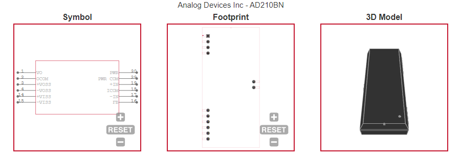 |
|
| FUNCTIONAL BLOCK DIAGRAM |
 |
|
| APPLICATIONS |
| • Multichannel Data Acquisition |
| • High Voltage Instrumentation Amplifier |
| • Current Shunt Measurements |
| • Process Signal Isolation |
|
| |