 |
| |
| ► 10 kΩ and 100 kΩ resistance options
|
| ► Resistor tolerance: 8% maximum
|
| ► Wiper current: ±6 mA
|
| ► Low temperature coefficient: 35 ppm/°C
|
| ► Wide bandwidth: 3 MHz |
| ► Fast start-up time < 75 µs
|
| ► Linear gain setting mode
|
| ► Single- and dual-supply operation |
| ► Independent logic supply: 1.8 V to 5.5 V
|
| ► Wide operating temperature: −40°C to +125°C |
| ► 3 mm × 3 mm LFCSP |
| ► Qualified for automotive applications |
| |
| CATALOG |
| AD5141BCPZ100-RL7 COUNTRY OF ORIGIN |
| AD5141BCPZ100-RL7 PARAMETRIC INFO |
| AD5141BCPZ100-RL7 PACKAGE INFO |
| AD5141BCPZ100-RL7 MANUFACTURING INFO |
| AD5141BCPZ100-RL7 PACKAGING INFO |
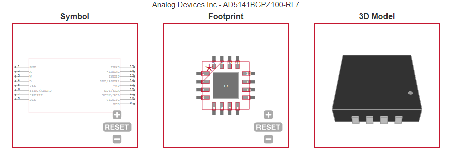
| AD5141BCPZ100-RL7 ECAD MODELS |
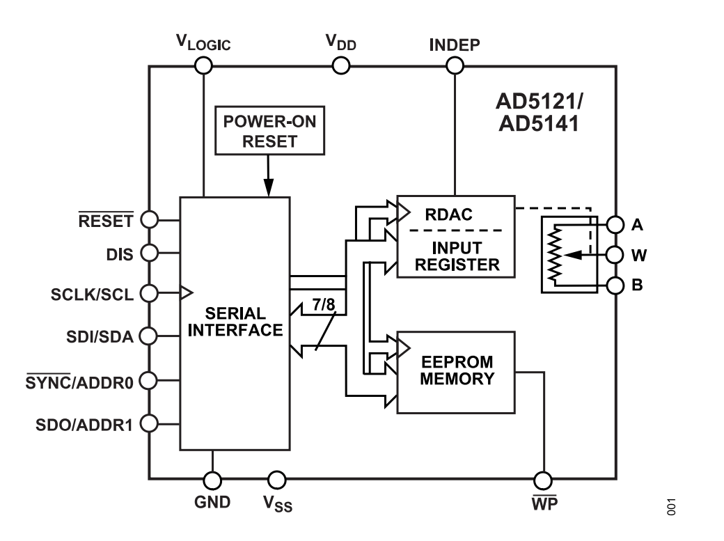
| AD5141BCPZ100-RL7 FUNCTIONAL BLOCK DIAGRAM |
| AD5141BCPZ100-RL7 APPLICATIONS
|
|
| COUNTRY OF ORIGIN |
| Korea (Republic of) |
| China |
| Philippines |
|
| PARAMETRIC INFO |
| Resistance Value (KOhm) |
100 |
| Number of Positions |
256 |
| Number of Pot per Package |
1 |
| Memory Type |
Non-Volatile |
| Taper Type |
Linear|Log |
| Minimum Operating Temperature (°C) |
-40 |
| Maximum Operating Temperature (°C) |
125 |
| Supplier Temperature Grade |
Extended Industrial |
| Power Supply Type |
Single|Dual |
| Maximum Dual Supply Voltage (V) |
±2.75 |
| Maximum Single Supply Voltage (V) |
5.5 |
| Maximum Supply Current (mA) |
0.0007(Typ) |
| Minimum Dual Supply Voltage (V) |
±2.25 |
| Minimum Single Supply Voltage (V) |
2.3 |
| Typical Dual Supply Voltage (V) |
±2.5 |
| Typical Single Supply Voltage (V) |
5 |
| Control Interface |
Serial (2-Wire, 4-Wire, I2C, SPI) |
| Maximum Storage Temperature (°C) |
150 |
| Minimum Storage Temperature (°C) |
-65 |
|
|
| PACKAGE INFO |
| Supplier Package |
LFCSP EP |
| Basic Package Type |
Non-Lead-Frame SMT |
| Pin Count |
16 |
| Lead Shape |
No Lead |
| PCB |
16 |
| Tab |
N/R |
| Pin Pitch (mm) |
0.5 |
| Package Length (mm) |
3 |
| Package Width (mm) |
3 |
| Package Height (mm) |
0.73 |
| Package Diameter (mm) |
N/R |
| Package Overall Length (mm) |
3 |
| Package Overall Width (mm) |
3 |
| Package Overall Height (mm) |
0.75 |
| Seated Plane Height (mm) |
0.75 |
| Mounting |
Surface Mount |
| Package Material |
Plastic |
| Package Description |
Lead Frame Chip Scale Package, Exposed Pad |
| Package Family Name |
CSP |
| Jedec |
MO-220WEED-6 |
| Package Outline |
Link to Datasheet |
|
|
| MANUFACTURING INFO |
| MSL |
3 |
| Maximum Reflow Temperature (°C) |
260 |
| Reflow Solder Time (Sec) |
30 |
| Number of Reflow Cycle |
3 |
| Standard |
J-STD-020D |
| Maximum Wave Temperature (°C) |
N/R |
| Wave Solder Time (Sec) |
N/R |
| Lead Finish(Plating) |
Matte Sn annealed |
| Under Plating Material |
Ag |
| Terminal Base Material |
Cu Alloy |
|
|
| PACKAGING INFO |
| Packaging Suffix |
RL7 |
| Packaging |
Tape and Reel |
| Quantity Of Packaging |
1500 |
| Reel Diameter (in) |
7 |
| Packaging Document |
Link to Datasheet |
|
|
| ECAD MODELS |
 |
|
| FUNCTIONAL BLOCK DIAGRAM |
 |
|
| APPLICATIONS
|
| ► Portable electronics level adjustment
|
| ► LCD panel brightness and contrast controls |
| ► Programmable filters, delays, and time constants
|
| ► Programmable power supplies
|
| |
| |