 |
|
| • 12-/16-bit resolution and monotonicity |
• Current output ranges: 4 mA to 20 mA, 0 mA to 20 mA, or
- 0 mA to 24 mA |
| • ±0.01% FSR typical total unadjusted error (TUE) |
| • ±3 ppm FSR/°C output drift |
• Voltage output ranges: 0 V to 5 V, 0 V to 10 V, ±5 V, or ±10 V
- 10% overrange
- ±0.01% FSR typical TUE
- ±2 ppm FSR/°C output drift |
| • Flexible serial digital interface |
| • On-chip output fault detection |
| • On-chip reference: 10 ppm/°C maximum |
| • Optional regulated DVCC output |
| • Asynchronous clear function |
• Power supply range
- AVDD: 10.8 V to 40 V
- AVSS: −26.4 V to −3 V/0 V |
| • Current loop compliance voltage: AVDD – 2.5 V |
| • Temperature range: −40°C to +105°C |
| • TSSOP and LFCSP packages |
|
| CATALOG |
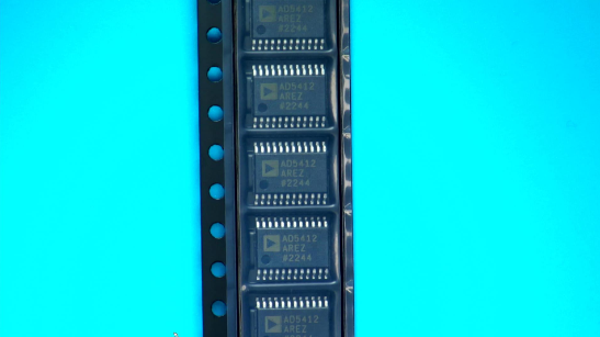
| AD5412AREZ-REEL7 COUNTRY OF ORIGIN |
| AD5412AREZ-REEL7 PARAMETRIC INFO |
| AD5412AREZ-REEL7 PACKAGE INFO |
| AD5412AREZ-REEL7 MANUFACTURING INFO |
| AD5412AREZ-REEL7 PACKAGING INFO |
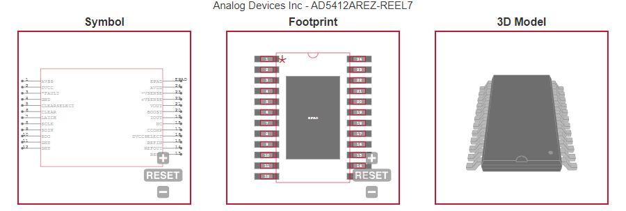
| AD5412AREZ-REEL7 ECAD MODELS |
| AD5412AREZ-REEL7 FUNCTIONAL BLOCK DIAGRAM |
| AD5412AREZ-REEL7 APPLICATIONS |
|
| COUNTRY OF ORIGIN |
| Ireland |
| Philippines |
|
| PARAMETRIC INFO |
| Architecture |
Segment |
| Resolution |
12bit |
| Number of DAC Channels |
1 |
| Number of Outputs per Chip |
1 |
| Conversion Rate |
40ksps |
| Converter Type |
General Purpose |
| Output Type |
Current|Voltage |
| Voltage Reference |
Internal|External |
| Maximum Settling Time (us) |
40(Typ)|25 |
| Digital Interface Type |
Serial (3-Wire, SPI, QSPI, Microwire) |
| Output Polarity |
Unipolar|Bipolar |
| Integral Nonlinearity Error |
±0.032%FSR |
| Full Scale Error |
±0.2%FSR |
| Minimum Operating Temperature (°C) |
-40 |
| Maximum Operating Temperature (°C) |
105 |
| Supplier Temperature Grade |
Industrial |
| Power Supply Type |
Single|Dual |
| Minimum Single Supply Voltage (V) |
10.8 |
| Typical Single Supply Voltage (V) |
12|15|18|24|28 |
| Maximum Single Supply Voltage (V) |
40 |
| Minimum Dual Supply Voltage (V) |
0/10.8 |
| Typical Dual Supply Voltage (V) |
±12|±15|±18|±24|±28 |
| Maximum Dual Supply Voltage (V) |
-26.4/40 |
| Digital Supply Support |
Yes |
| Maximum Power Dissipation (mW) |
128(Typ) |
|
| |
| PACKAGE INFO |
| Supplier Package |
TSSOP EP |
| Basic Package Type |
Lead-Frame SMT |
| Pin Count |
24 |
| Lead Shape |
Gull-wing |
| PCB |
24 |
| Tab |
N/R |
| Pin Pitch (mm) |
0.65 |
| Package Length (mm) |
7.8 |
| Package Width (mm) |
4.4 |
| Package Height (mm) |
1 |
| Package Diameter (mm) |
N/R |
| Seated Plane Height (mm) |
1.2(Max) |
| Mounting |
Surface Mount |
| Package Material |
Plastic |
| Package Description |
Thin Shrink Small Outline Package, Exposed Pad |
| Package Family Name |
SO |
| Jedec |
MO-153AD |
| Package Outline |
Link to Datasheet |
|
| |
| MANUFACTURING INFO |
| MSL |
3 |
| Maximum Reflow Temperature (°C) |
260 |
| Reflow Solder Time (Sec) |
30 |
| Number of Reflow Cycle |
3 |
| Standard |
J-STD-020D |
| Maximum Wave Temperature (°C) |
N/R |
| Wave Solder Time (Sec) |
N/R |
| Lead Finish(Plating) |
Matte Sn annealed |
| Under Plating Material |
N/A |
| Terminal Base Material |
Cu Alloy |
|
| |
| PACKAGING INFO |
| Packaging Suffix |
REEL7 |
| Packaging |
Tape and Reel |
| Quantity Of Packaging |
1000 |
| Reel Diameter (in) |
7 |
| Packaging Document |
Link to Datasheet |
|
| |
| ECAD MODELS |
 |
|
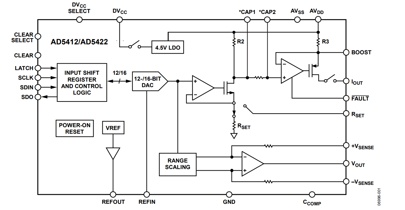
| FUNCTIONAL BLOCK DIAGRAM |
 |
|
| APPLICATIONS |
| • Process controls |
| • Actuator controls |
| • PLC |
| • HART network connectivity (LFCSP package only) |
|