
|
| |
• 16-bit resolution
|
• 11.8 nV/√Hz noise spectral density
|
• 1 µs settling time
|
| • 1.1 nV-sec glitch energy |
| • 0.05 ppm/°C temperature drift |
| • 5 kV HBM ESD classification |
| • 0.375 mW power consumption at 3 V |
| • 2.7 V to 5.5 V single-supply operation |
| • Hardware CS and LDAC functions |
| • 50 MHz SPI-/QSPI-/MICROWIRE-/DSP-compatible interface |
| • Power-on reset clears DAC output to zero scale |
| • Available in 3 mm × 3 mm, 8-/10-lead LFCSP and 10-lead MSOP |
| |
| CATALOG |
| AD5541ABRMZ COUNTRY OF ORIGIN |
AD5541ABRMZ PARAMETRIC INFO
|
AD5541ABRMZ PACKAGE INFO
|
AD5541ABRMZ MANUFACTURING INFO
|
AD5541ABRMZ PACKAGING INFO
|
| AD5541ABRMZ FUNCTIONAL BLOCK DIAGRAMS |
AD5541ABRMZ EACD MODELS
|
| AD5541ABRMZ APPLICATIONS |
|
| COUNTRY OF ORIGIN |
| Taiwan (Province of China) |
| |
PARAMETRIC INFO
|
| Architecture |
Segment |
| Resolution |
16bit |
| Number of DAC Channels |
1 |
| Number of Outputs per Chip |
1 |
| Converter Type |
General Purpose |
| Output Type |
Voltage |
| Voltage Reference |
External |
| Maximum Settling Time (us) |
1(Typ) |
| Digital Interface Type |
Serial (3-Wire, 4-Wire, SPI, QSPI, Microwire) |
| Output Polarity |
Unipolar |
| Integral Nonlinearity Error |
±1LSB |
| Full Scale Error |
±4LSB |
| Signal to Noise Ratio |
92dB(Typ) |
| Minimum Operating Temperature (°C) |
-40 |
| Maximum Operating Temperature (°C) |
125 |
| Supplier Temperature Grade |
Industrial |
| Power Supply Type |
Single |
| Minimum Single Supply Voltage (V) |
2.7 |
| Typical Single Supply Voltage (V) |
5 |
| Maximum Single Supply Voltage (V) |
5.5 |
| Digital Supply Support |
No |
| Maximum Power Dissipation (mW) |
0.825 |
|
|
PACKAGE INFO
|
| Supplier Package |
MSOP |
| Basic Package Type |
Lead-Frame SMT |
| Pin Count |
10 |
| Lead Shape |
Gull-wing |
| PCB |
10 |
| Tab |
N/R |
| Pin Pitch (mm) |
0.5 |
| Package Length (mm) |
3 |
| Package Width (mm) |
3 |
| Package Height (mm) |
0.85 |
| Package Diameter (mm) |
N/R |
| Package Overall Length (mm) |
3 |
| Package Overall Width (mm) |
4.9 |
| Package Overall Height (mm) |
1.1(Max) |
| Seated Plane Height (mm) |
1.1(Max) |
| Mounting |
Surface Mount |
| Package Weight (g) |
N/A |
| Package Material |
Plastic |
| Package Description |
Micro Small Outline Package |
| Package Family Name |
SO |
| Jedec |
MO-187BA |
| Package Outline |
Link to Datasheet |
|
|
MANUFACTURING INFO
|
| MSL |
1 |
| Maximum Reflow Temperature (°C) |
260 |
| Reflow Solder Time (Sec) |
30 |
| Number of Reflow Cycle |
3 |
| Standard |
J-STD-020D |
| Maximum Wave Temperature (°C) |
N/R |
| Wave Solder Time (Sec) |
N/R |
| Lead Finish(Plating) |
Matte Sn annealed |
| Under Plating Material |
Ag |
| Terminal Base Material |
Cu Alloy |
|
|
PACKAGING INFO
|
| Packaging |
Tube |
| Quantity Of Packaging |
50 |
| Packaging Document |
Link to Datasheet |
|
|
| FUNCTIONAL BLOCK DIAGRAMS |
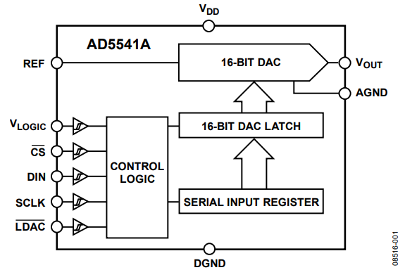 |
| |
ECAD MODELS
|
|
|
| APPLICATIONS |
| • Automatic test equipment |
| • Precision source-measure instruments |
| • Data acquisition systems |
| • Medical instrumentation |
| • Aerospace instrumentation |
| • Communications infrastructure equipment |
| • Industrial control |
|