 |
||||||||||||||||||||||||||||||||||||
| |
||||||||||||||||||||||||||||||||||||
| • Easy to use - Gain set with one external resistor - (Gain range 1 to 10,000) - Wide power supply range (±2.3 V to ±18 V) - Higher performance than 3 op amp IA designs - Available in 8-lead DIP and SOIC packaging - Low power, 1.3 mA max supply current |
||||||||||||||||||||||||||||||||||||
| • Excellent dc performance (B grade) - 50 μV max, input offset voltage - 0.6 μV/°C max, input offset drift - 1.0 nA max, input bias current - 100 dB min common-mode rejection ratio (G = 10) |
||||||||||||||||||||||||||||||||||||
| • Low noise - 9 nV/√Hz @ 1 kHz, input voltage noise - 0.28 μV p-p noise (0.1 Hz to 10 Hz) |
||||||||||||||||||||||||||||||||||||
| • Excellent ac specifications - 120 kHz bandwidth (G = 100) - 15 μs settling time to 0.01% |
||||||||||||||||||||||||||||||||||||
| |
||||||||||||||||||||||||||||||||||||
| CATALOG | ||||||||||||||||||||||||||||||||||||
| AD620SQ/883B COUNTRY OF ORIGIN | ||||||||||||||||||||||||||||||||||||
| AD620SQ/883B PARAMETRIC INFO | ||||||||||||||||||||||||||||||||||||
| AD620SQ/883B PACKAGE INFO | ||||||||||||||||||||||||||||||||||||
| AD620SQ/883B MANUFACTURING INFO | ||||||||||||||||||||||||||||||||||||
| AD620SQ/883B PACKAGING INFO | ||||||||||||||||||||||||||||||||||||
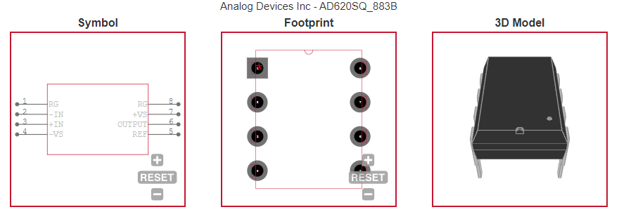
| AD620SQ/883B ECAD MODELS | ||||||||||||||||||||||||||||||||||||
| AD620SQ/883B APPLICATIONS | ||||||||||||||||||||||||||||||||||||
| |
||||||||||||||||||||||||||||||||||||
| COUNTRY OF ORIGIN | ||||||||||||||||||||||||||||||||||||
| Taiwan (Province of China) | ||||||||||||||||||||||||||||||||||||
| Philippines | ||||||||||||||||||||||||||||||||||||
| |
||||||||||||||||||||||||||||||||||||
| PARAMETRIC INFO | ||||||||||||||||||||||||||||||||||||
|
||||||||||||||||||||||||||||||||||||
| |
||||||||||||||||||||||||||||||||||||
| PACKAGE INFO | ||||||||||||||||||||||||||||||||||||
|
||||||||||||||||||||||||||||||||||||
| |
||||||||||||||||||||||||||||||||||||
| MANUFACTURING INFO | ||||||||||||||||||||||||||||||||||||
|
||||||||||||||||||||||||||||||||||||
| |
||||||||||||||||||||||||||||||||||||
| PACKAGING INFO | ||||||||||||||||||||||||||||||||||||
|
||||||||||||||||||||||||||||||||||||
| |
||||||||||||||||||||||||||||||||||||
| ECAD MODELS | ||||||||||||||||||||||||||||||||||||
 |
||||||||||||||||||||||||||||||||||||
| |
||||||||||||||||||||||||||||||||||||
| APPLICATIONS | ||||||||||||||||||||||||||||||||||||
| • Weigh scales | ||||||||||||||||||||||||||||||||||||
| • ECG and medical instrumentation | ||||||||||||||||||||||||||||||||||||
| • Transducer interface | ||||||||||||||||||||||||||||||||||||
| • Data acquisition systems | ||||||||||||||||||||||||||||||||||||
| • Industrial process controls | ||||||||||||||||||||||||||||||||||||
| • Battery-powered and portable equipment | ||||||||||||||||||||||||||||||||||||