 |
|
| • Improved replacement for: INA117P and INA117KU |
| • ±270 V common-mode voltage range |
• Input protection to
±500 V common mode
±500 V differential mode |
| • Wide power supply range (±2.5 V to ±18 V) |
| • ±10 V output swing on ±12 V supply |
| • 1 mA maximum power supply current |
| • HIGH ACCURACY DC PERFORMANCE |
| • 3 ppm maximum gain nonlinearity (AD629B) |
| • 20 μV/°C maximum offset drift (AD629A) |
| • 10 μV/°C maximum offset drift (AD629B) |
| • 10 ppm/°C maximum gain drift |
| • EXCELLENT AC SPECIFICATIONS |
| • 77 dB minimum CMRR @ 500 Hz (AD629A) |
| • 86 dB minimum CMRR @ 500 Hz (AD629B) |
| • 500 kHz bandwidth |
|
| CATALOG |
| AD629ARZ-R7 COUNTRY OF ORIGIN |
| AD629ARZ-R7 PARAMETRIC INFO |
| AD629ARZ-R7 PACKAGE INFO |
| AD629ARZ-R7 MANUFACTURING INFO |
| AD629ARZ-R7 PACKAGING INFO |
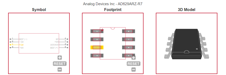
| AD629ARZ-R7 ECAD MODELS |
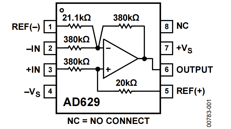
| AD629ARZ-R7 FUNCTIONAL BLOCK DIAGRAM |
| AD629ARZ-R7 APPLICATIONS |
|
| COUNTRY OF ORIGIN |
| China |
| United States of America |
|
| PARAMETRIC INFO |
| Type |
Differential Amplifier |
| Number of Elements per Chip |
1 |
| Number of Channels per Chip |
1 |
| Minimum PSRR (dB) |
84 |
| Maximum Input Offset Voltage (mV) |
1@±15V |
| Minimum CMRR (dB) |
77 |
| Maximum Quiescent Current (mA) |
1@±15V |
| Minimum CMRR Range (dB) |
75 to 85 |
| Maximum Input Resistance (MOhm) |
0.8(Typ)@±15V |
| Maximum Voltage Gain Range (dB) |
<35 |
| Maximum Voltage Gain (dB) |
0(Typ) |
| Minimum Operating Temperature (°C) |
-40 |
| Maximum Operating Temperature (°C) |
85 |
| Supplier Temperature Grade |
Industrial |
| Power Supply Type |
Dual |
| Maximum Supply Voltage Range (V) |
30 to 50 |
| Minimum Dual Supply Voltage (V) |
±2.5 |
| Typical Dual Supply Voltage (V) |
±3|±5|±9|±12|±15 |
| Maximum Dual Supply Voltage (V) |
±18 |
| Maximum Operating Supply Voltage (V) |
±18 |
|
| PACKAGE INFO |
| Supplier Package |
SOIC N |
| Basic Package Type |
Lead-Frame SMT |
| Pin Count |
8 |
| Lead Shape |
Gull-wing |
| PCB |
8 |
| Tab |
N/R |
| Pin Pitch (mm) |
1.27 |
| Package Length (mm) |
5(Max) |
| Package Width (mm) |
4(Max) |
| Package Height (mm) |
1.5(Max) |
| Package Diameter (mm) |
N/R |
| Package Overall Length (mm) |
5(Max) |
| Package Overall Width (mm) |
6.2(Max) |
| Package Overall Height (mm) |
1.75(Max) |
| Seated Plane Height (mm) |
1.75(Max) |
| Mounting |
Surface Mount |
| Package Weight (g) |
N/A |
| Package Material |
Plastic |
| Package Description |
Small Outline IC Narrow Body |
| Package Family Name |
SO |
| Jedec |
MS-012AA |
| Package Outline |
Link to Datasheet |
|
| MANUFACTURING INFO |
| MSL |
1 |
| Maximum Reflow Temperature (°C) |
260 |
| Reflow Solder Time (Sec) |
30 |
| Number of Reflow Cycle |
3 |
| Standard |
J-STD-020D |
| Maximum Wave Temperature (°C) |
300 |
| Wave Solder Time (Sec) |
60 |
| Wave Temp. Source |
Link to Datasheet |
| Lead Finish(Plating) |
Matte Sn annealed |
| Under Plating Material |
Ag |
| Terminal Base Material |
Cu Alloy |
|
| PACKAGING INFO |
| Packaging Suffix |
R7 |
| Packaging |
Tape and Reel |
| Quantity Of Packaging |
1000 |
| Reel Diameter (in) |
7 |
| Tape Pitch (mm) |
8 |
| Tape Width (mm) |
12 |
| Component Orientation |
Q1 |
| Packaging Document |
Link to Datasheet |
| Tape Material |
Plastic |
| Tape Type |
Embossed |
|
| ECAD MODELS |
 |
|
| FUNCTIONAL BLOCK DIAGRAM |
|
|
| APPLICATIONS |
| • High voltage current sensing |
| • Battery cell voltage monitors |
| • Power supply current monitors |
| • Motor controls |
| • Isolation |
|