 |
||||||||||||||||||||||||||||||
| |
||||||||||||||||||||||||||||||
| • High instantaneous dynamic range - Noise figure (NF) as low as 13 dB - Noise spectral density (NSD) as low as −159 dBFS/Hz - IIP3 up to 36.9 dBm with spurious tones <−99 dBFS |
||||||||||||||||||||||||||||||
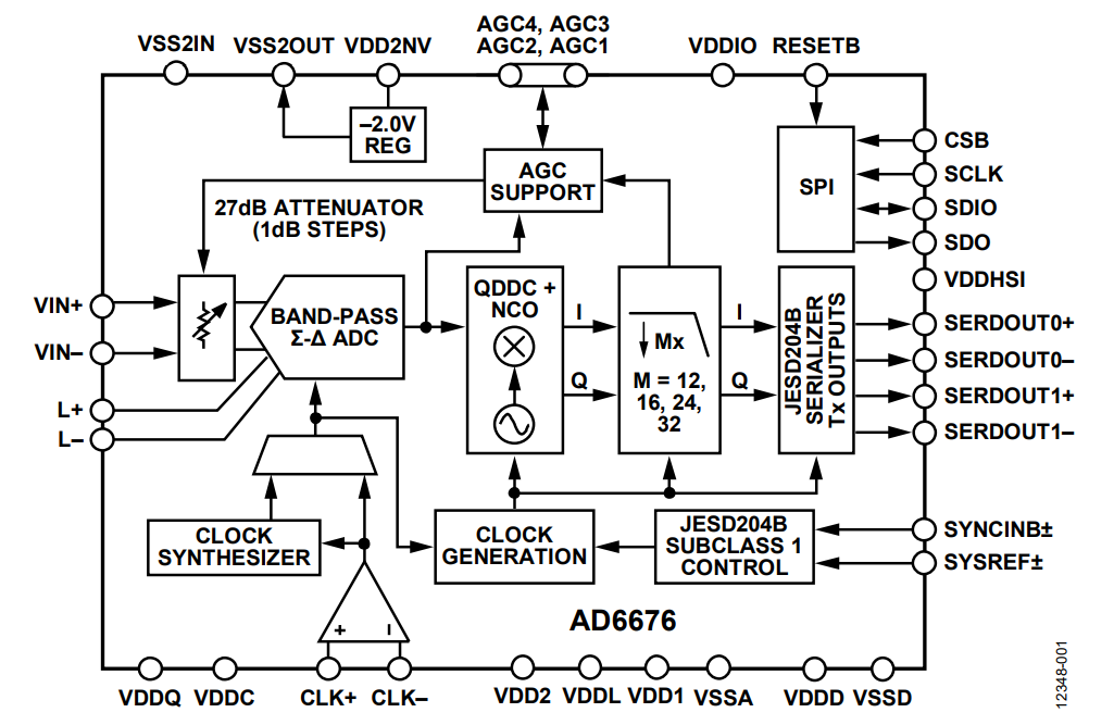
| • Tunable band-pass Σ-Δ analog-to-digital converter (ADC) - 20 MHz to 160 MHz signal bandwidth - 70 MHz to 450 MHz IF center frequency - Configurable input full-scale level of −2 dBm to −14 dBm Easy to drive resistive IF input - Gain flatness of 1 dB with under 0.5 dB out-of-band peaking Alias rejection greater than 50 dB - 2.0 GSPS to 3.2 GSPS ADC clock rate On-chip PLL clock multiplier - 16-bit I/Q rate up to 266 MSPS |
||||||||||||||||||||||||||||||
| • On-chip digital signal processing - NCO and quadrature digital downconverter (QDDC) - Selectable decimation factor of 12, 16, 24, and 32 |
||||||||||||||||||||||||||||||
| • Automatic gain control (AGC) support - On-chip attenuator with 27 dB span in 1 dB steps - Fast attenuator control via configurable AGC data port - Peak detection flags with programmable thresholds |
||||||||||||||||||||||||||||||
| • Single or dual lane, JESD204B capable | ||||||||||||||||||||||||||||||
| • Low power consumption: 1.20 W - 1.1 V and 2.5 V supply voltage - TDD power saving up to 60% |
||||||||||||||||||||||||||||||
| • 4.3 mm × 5.0 mm WLCSP | ||||||||||||||||||||||||||||||
| CATALOG | ||||||||||||||||||||||||||||||
| AD6676BCBZRL COUNTRY OF ORIGIN | ||||||||||||||||||||||||||||||
| AD6676BCBZRL PARAMETRIC INFO | ||||||||||||||||||||||||||||||
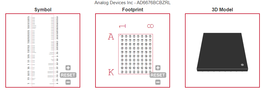
| AD6676BCBZRL PACKAGE INFO | ||||||||||||||||||||||||||||||
| AD6676BCBZRL MANUFACTURING INFO | ||||||||||||||||||||||||||||||
| AD6676BCBZRL PACKAGING INFO | ||||||||||||||||||||||||||||||
| AD6676BCBZRL ECAD MODELS | ||||||||||||||||||||||||||||||
| AD6676BCBZRL FUNCTIONAL BLOCK DIAGRAM | ||||||||||||||||||||||||||||||
| AD6676BCBZRL APPLICATIONS | ||||||||||||||||||||||||||||||
| |
||||||||||||||||||||||||||||||
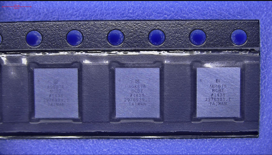
| COUNTRY OF ORIGIN | ||||||||||||||||||||||||||||||
| Taiwan (Province of China) | ||||||||||||||||||||||||||||||
| |
||||||||||||||||||||||||||||||
| PARAMETRIC INFO | ||||||||||||||||||||||||||||||
|
||||||||||||||||||||||||||||||
| PACKAGE INFO | ||||||||||||||||||||||||||||||
|
||||||||||||||||||||||||||||||
| MANUFACTURING INFO | ||||||||||||||||||||||||||||||
|
||||||||||||||||||||||||||||||
| PACKAGING INFO | ||||||||||||||||||||||||||||||
|
||||||||||||||||||||||||||||||
| ECAD MODELS | ||||||||||||||||||||||||||||||
 |
||||||||||||||||||||||||||||||
| |
||||||||||||||||||||||||||||||
| FUNCTIONAL BLOCK DIAGRAM | ||||||||||||||||||||||||||||||
 |
||||||||||||||||||||||||||||||
| |
||||||||||||||||||||||||||||||
| APPLICATIONS | ||||||||||||||||||||||||||||||
| • Wideband cellular infrastructure equipment and repeaters | ||||||||||||||||||||||||||||||
| • Point-to-point microwave equipment | ||||||||||||||||||||||||||||||
| • Instrumentation - Spectrum and communication analyzers |
||||||||||||||||||||||||||||||
| • Software defined radio | ||||||||||||||||||||||||||||||
| |