|
|
• 16-bit resolution with no missing codes
|
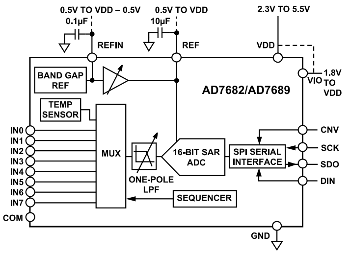
• 4-channel (AD7682)/8-channel (AD7689) multiplexer with choice
of inputs
|
• Unipolar single-ended
|
• Differential (GND sense)
|
• Pseudobipolar
|
| • Throughput: 250 kSPS |
| • INL: ±0.4 LSB typical, ±1.5 LSB maximum (±23 ppm or FSR) |
| • Dynamic range: 93.8 dB |
| • SINAD: 92.5 dB at 20 kHz |
| • THD: −100 dB at 20 kHz |
| • Analog input range: 0 V to VREF with VREF up to VDD
|
| • Multiple reference types
► Internal selectable 2.5 V or 4.096 V
► External buffered (up to 4.096 V)
► External (up to VDD)
|
| • Internal temperature sensor (TEMP)
|
| • Channel sequencer, selectable 1-pole filter, busy indicator |
| • No pipeline delay, SAR architecture
|
| • Single-supply 2.3 V to 5.5 V operation with 1.8 V to 5.5 V logic
interface |
| • Serial interface compatible with SPI, MICROWIRE, QSPI, and
DSP
|
|
| CATALOG |
AD7689BCPZRL7 COUNTRY OF ORIGIN
|
AD7689BCPZRL7 PARAMETRIC INFO
|
AD7689BCPZRL7 PACKAGE INFO
|
AD7689BCPZRL7 MANUFACTURING INFO
|
AD7689BCPZRL7 PACKAGING INFO
|
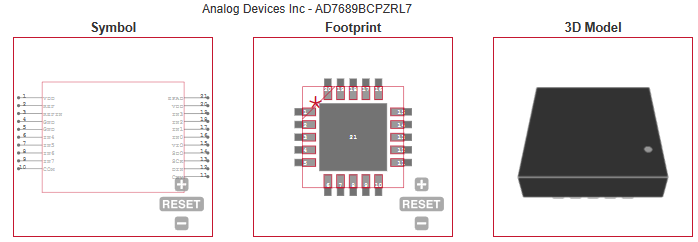
AD7689BCPZRL7 ECAD MODELS
|
| AD7689BCPZRL7 FUNCTIONAL BLOCK DIAGRAM |
AD7689BCPZRL7 APPLICATIONS
|
|
COUNTRY OF ORIGIN
|
| China |
| Korea (Republic of) |
| Philippines |
|
PARAMETRIC INFO
|
| Converter Type |
General Purpose |
| Input Type |
Voltage |
| Architecture |
SAR |
| Resolution |
16bit |
| Number of ADCs |
1 |
| Sampling Rate |
250ksps |
| Digital Interface Type |
Serial (4-Wire, SPI, QSPI, Microwire) |
| Voltage Reference |
Internal|External |
| Input Signal Type |
Single-Ended|Pseudo-Differential|Differential |
| Polarity of Input Voltage |
Unipolar|Bipolar |
| Minimum Operating Temperature (°C) |
-40 |
| Maximum Operating Temperature (°C) |
85 |
| Integral Nonlinearity Error |
±2LSB |
| Signal to Noise Ratio |
93.8dB(Typ) |
| Sample and Hold |
Yes |
| Number of Input Channels |
8|8/4|4/2 |
| Single-Ended Input |
Yes |
| Differential Input |
Yes |
| Input Voltage |
2.5V/4.096V|±1.25V/±2.048V |
| No Missing Codes (bit) |
16 |
| Full Scale Error |
±8LSB |
| Differential Nonlinearity |
-1/1.5LSB |
| Voltage Supply Source |
Single |
| Minimum Single Supply Voltage (V) |
2.3 |
| Typical Single Supply Voltage (V) |
2.5|3.3|5 |
| Maximum Single Supply Voltage (V) |
5.5 |
| Digital Supply Support |
No |
| Typical Power Dissipation (mW) |
15.5 |
| Maximum Power Dissipation (mW) |
21 |
|
|
PACKAGE INFO
|
| Supplier Package |
LFCSP EP |
| Basic Package Type |
Non-Lead-Frame SMT |
| Pin Count |
20 |
| Lead Shape |
No Lead |
| PCB |
20 |
| Tab |
N/R |
| Pin Pitch (mm) |
0.5 |
| Package Length (mm) |
4 |
| Package Width (mm) |
4 |
| Package Height (mm) |
0.73 |
| Package Diameter (mm) |
N/R |
| Package Overall Length (mm) |
4 |
| Package Overall Width (mm) |
4 |
| Package Overall Height (mm) |
0.75 |
| Seated Plane Height (mm) |
0.75 |
| Mounting |
Surface Mount |
| Package Weight (g) |
N/A |
| Package Material |
Plastic |
| Package Description |
Lead Frame Chip Scale Package, Exposed Pad |
| Package Family Name |
CSP |
| Jedec |
MO-220-WGGD |
|
|
MANUFACTURING INFO
|
| MSL |
3 |
| Maximum Reflow Temperature (°C) |
260 |
| Reflow Solder Time (Sec) |
30 |
| Number of Reflow Cycle |
3 |
| Standard |
J-STD-020D |
| Maximum Wave Temperature (°C) |
N/R |
| Wave Solder Time (Sec) |
N/R |
| Lead Finish(Plating) |
Matte Sn annealed |
| Under Plating Material |
Ag |
| Terminal Base Material |
Cu Alloy |
| Number of Wave Cycles |
N/R |
|
|
PACKAGING INFO
|
| Packaging Suffix |
RL7 |
| Packaging |
Tape and Reel |
| Quantity Of Packaging |
1500 |
| Reel Diameter (in) |
7 |
| Packaging Document |
Link to Datasheet |
|
|
ECAD MODELS
|
|
|
FUNCTIONAL BLOCK DIAGRAM
|
|
|
APPLICATIONS
|
• Multichannel system monitoring
|
| • Battery-powered equipment
|
• Medical instruments: ECG/EKG
|
• Mobile communications: GPS
|
• Power line monitoring
|
| • Data acquisition |
| • Seismic data acquisition systems |
| • Instrumentation |
| • Process control
|
| |