|
|
• Low power: 40 μA supply current (maximum)
|
• Low input currents
- 1 pA input bias current
- 0.5 pA input offset current
|
• High CMRR: 110 dB CMRR, G = 100
|
• Space-saving MSOP
|
• Zero input crossover distortion
|
• Rail-to-rail input and output
|
• Gain set with single resistor
|
• Operates from 1.8 V to 5.5 V
|
|
| CATALOG |
AD8236ARMZ-R7 Country of Origin
|
AD8236ARMZ-R7 Parametric Info
|
AD8236ARMZ-R7 Package Info
|
AD8236ARMZ-R7 Manufacturing Info
|
AD8236ARMZ-R7 Packaging Info
|
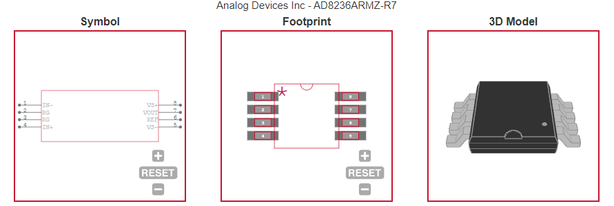
AD8236ARMZ-R7 ECAD Models
|
| AD8236ARMZ-R7 APPLICATIONS |
|
COUNTRY OF ORIGIN
|
Malaysia
|
|
PARAMETRIC INFO
|
| Rail to Rail |
Rail to Rail Input/Output |
| Number of Channels per Chip |
1 |
| Maximum Input Offset Voltage (mV) |
3.5@5V |
| Maximum Input Bias Current (uA) |
0.00001@5V |
| Minimum CMRR (dB) |
86 |
| Maximum Quiescent Current (mA) |
0.04@1.8V |
| Minimum CMRR Range (dB) |
75 to 85 |
| Minimum Single Supply Voltage (V) |
1.8 |
| Maximum Single Supply Voltage (V) |
5.5 |
| Maximum Input Resistance (MOhm) |
440000@5V |
| Maximum Voltage Gain Range (dB) |
35 to 50 |
| Maximum Voltage Gain (dB) |
46.02 |
| Minimum Operating Temperature (°C) |
-40 |
| Maximum Operating Temperature (°C) |
125 |
| Supplier Temperature Grade |
Industrial |
| Power Supply Type |
Single |
| Maximum Supply Voltage Range (V) |
<5 |
| Typical Single Supply Voltage (V) |
3|5 |
| Maximum Operating Supply Voltage (V) |
5.5 |
|
|
PACKAGE INFO
|
| Supplier Package |
MSOP |
| Basic Package Type |
Lead-Frame SMT |
| Pin Count |
8 |
| Lead Shape |
Gull-wing |
| PCB |
8 |
| Tab |
N/R |
| Pin Pitch (mm) |
0.65 |
| Package Length (mm) |
3 |
| Package Width (mm) |
3 |
| Package Height (mm) |
0.85 |
| Package Diameter (mm) |
N/R |
| Package Overall Length (mm) |
3 |
| Package Overall Width (mm) |
4.9 |
| Package Overall Height (mm) |
1.1(Max) |
| Seated Plane Height (mm) |
1.1(Max) |
| Mounting |
Surface Mount |
| Package Weight (g) |
N/A |
| Package Material |
Plastic |
| Package Description |
Micro Small Outline Package |
| Package Family Name |
SO |
| Jedec |
MO-187AA |
| Package Outline |
Link to Datasheet |
|
|
MANUFACTURING INFO
|
| MSL |
1 |
| Maximum Reflow Temperature (°C) |
260 |
| Reflow Solder Time (Sec) |
30 |
| Number of Reflow Cycle |
3 |
| Standard |
J-STD-020D |
| Maximum Wave Temperature (°C) |
N/R |
| Wave Solder Time (Sec) |
N/R |
| Lead Finish(Plating) |
Au |
| Under Plating Material |
Pd over Ni |
| Terminal Base Material |
Cu Alloy |
| Number of Wave Cycles |
N/R |
|
|
PACKAGING INFO
|
| Packaging Suffix |
R7 |
| Packaging |
Tape and Reel |
| Quantity Of Packaging |
1000 |
| Reel Diameter (in) |
7 |
| Packaging Document |
Link to Datasheet |
|
|
ECAD MODELS
|
|
|
APPLICATIONS
|
• Medical instrumentation
|
• Low-side current sense
|
• Portable devices
|
|
|