|
|
• Lowest auto-zero amplifier noise
|
• Low offset voltage: 1 µV
|
• Input offset drift: 0.002 µV/°C
|
• Rail-to-rail input and output swing
|
• 5 V single-supply operation
|
• High gain, CMRR, and PSRR: 130 dB
|
• Very low input bias current: 100 pA maximum
|
• Low supply current: 1.0 mA
|
• Overload recovery time: 50 µs
|
• No external components required
|
• Qualified for automotive applications
|
|
| CATALOG |
AD8630ARUZ-REEL COUNTRY OF ORIGIN
|
AD8630ARUZ-REEL PARAMETRIC INFO
|
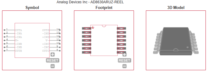
AD8630ARUZ-REEL PACKAGE INFO
|
AD8630ARUZ-REEL MANUFACTURING INFO
|
AD8630ARUZ-REEL PACKAGING INFO
|
AD8630ARUZ-REEL ECAD MODELS
|
AD8630ARUZ-REEL APPLICATIONS
|
|
COUNTRY OF ORIGIN
|
Malaysia
|
Philippines
|
Taiwan (Province of China)
|
|
PARAMETRIC INFO
|
| Manufacturer Type |
Zero Drift Amplifier |
| Type |
Auto Zero/Chopper |
| Rail to Rail |
Rail to Rail Input/Output |
| Minimum Single Supply Voltage (V) |
2.7 |
| Number of Channels per Chip |
4 |
| Minimum PSRR (dB) |
115 |
| Typical Single Supply Voltage (V) |
3 |
| Maximum Single Supply Voltage (V) |
5 |
| Minimum Dual Supply Voltage (V) |
±1.35 |
| Typical Gain Bandwidth Product (MHz) |
2.5 |
| Maximum Input Offset Voltage (mV) |
0.005@5V |
| Maximum Input Offset Current (uA) |
0.0002@5V |
| Maximum Dual Supply Voltage (V) |
±2.5 |
| Maximum Operating Supply Voltage (V) |
±2.5|5 |
| Maximum Input Bias Current (uA) |
0.0003@5V |
| Minimum CMRR (dB) |
120 |
| Maximum Supply Voltage Range (V) |
<5.5 |
| Minimum CMRR Range (dB) |
>=115 |
| Typical Voltage Gain (dB) |
145 |
| Typical Slew Rate (V/us) |
1@5V |
| Typical Output Current (mA) |
30@5V |
| Typical Input Noise Voltage Density (nV/rtHz) |
22@5V |
| Typical Noninverting Input Current Noise Density (pA/rtHz) |
0.005@5V |
| Typical Input Bias Current (uA) |
0.0001@5V |
| Shut Down Support |
No |
| Minimum Operating Temperature (°C) |
-40 |
| Maximum Operating Temperature (°C) |
125 |
| Supplier Temperature Grade |
Extended Industrial |
| Minimum Storage Temperature (°C) |
-65 |
| Maximum Storage Temperature (°C) |
150 |
| Power Supply Type |
Single|Dual |
| Maximum Supply Current (mA) |
4.4@5V |
| Typical Low Level Output Voltage (V) |
0.001 |
| Input Offset Voltage Drift (uV/°C) |
0.02 |
|
|
PACKAGE INFO
|
| Supplier Package |
TSSOP |
| Basic Package Type |
Lead-Frame SMT |
| Pin Count |
14 |
| Lead Shape |
Gull-wing |
| PCB |
14 |
| Tab |
N/R |
| Pin Pitch (mm) |
0.65 |
| Package Length (mm) |
5 |
| Package Width (mm) |
4.4 |
| Package Height (mm) |
1 |
| Package Diameter (mm) |
N/R |
| Package Overall Length (mm) |
5 |
| Package Overall Width (mm) |
6.4 |
| Package Overall Height (mm) |
1.2(Max) |
| Seated Plane Height (mm) |
1.2(Max) |
| Mounting |
Surface Mount |
| Package Weight (g) |
N/A |
| Package Material |
Plastic |
| Package Description |
Thin Shrink Small Outline Package |
| Package Family Name |
SOP |
| Jedec |
MO-153AB-1 |
| Package Outline |
Link to Datasheet |
|
|
MANUFACTURING INFO
|
| MSL |
1 |
| Maximum Reflow Temperature (°C) |
260 |
| Reflow Solder Time (Sec) |
30 |
| Number of Reflow Cycle |
3 |
| Standard |
J-STD-020D |
| Maximum Wave Temperature (°C) |
300 |
| Wave Solder Time (Sec) |
60 |
| Wave Temp. Source |
Link to Datasheet |
| Lead Finish(Plating) |
Matte Sn annealed |
| Under Plating Material |
Ag |
| Terminal Base Material |
Cu Alloy |
|
|
PACKAGING INFO
|
| Packaging Suffix |
REEL |
| Packaging |
Tape and Reel |
| Quantity Of Packaging |
2500 |
|
|
ECAD MODELS
|
|
|
APPLICATIONS
|
• Automotive sensors
|
| • Pressure and position sensors |
| • Strain gage amplifiers |
| • Medical instrumentation |
• Thermocouple amplifiers
|
• Precision current sensing
|
• Photodiode amplifiers
|
| |