|
|
• 1.8 V analog supply operation
|
• 1.8 V CMOS or LVDS outputs
|
• SNR = 74.5 dBFS @ 70 MHz
|
• SFDR = 91 dBc @ 70 MHz
|
• Low power: 106 mW/channel @ 125 MSPS
|
• Differential analog input with 650 MHz bandwidth
|
• IF sampling frequencies to 200 MHz
|
• On-chip voltage reference and sample-and-hold circuit
|
• 2 V p-p differential analog input
|
• DNL = ±0.5 LSB
|
|
| CATALOG |
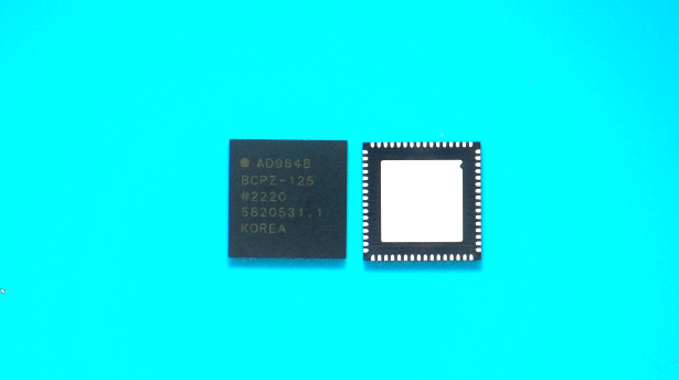
| AD9648BCPZ-125 COUNTRY OF ORIGIN |
AD9648BCPZ-125 PARAMETRIC INFO
|
AD9648BCPZ-125 PACKAGE INFO
|
AD9648BCPZ-125 MANUFACTURING INFO
|
AD9648BCPZ-125 PACKAGING INFO
|
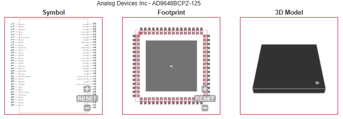
AD9648BCPZ-125 ECAD MODELS
|
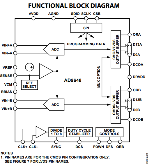
AD9648BCPZ-125 FUNCTIONAL BLOCK DIAGRAM
|
AD9648BCPZ-125 APPLICATIONS
|
|
COUNTRY OF ORIGIN
|
| Korea (Republic of) |
Malaysia
|
Singapore
|
Taiwan (Province of China)
|
|
PARAMETRIC INFO
|
| Converter Type |
General Purpose |
| Input Type |
Voltage |
| Architecture |
Pipelined |
| Resolution |
14bit |
| Number of ADCs |
2 |
| Sampling Rate |
125Msps |
| Digital Interface Type |
Parallel |
| Voltage Reference |
Internal|External |
| Input Signal Type |
Differential |
| Polarity of Input Voltage |
Unipolar|Bipolar |
| Minimum Operating Temperature (°C) |
-40 |
| Maximum Operating Temperature (°C) |
85 |
| Supplier Temperature Grade |
Industrial |
| Minimum Storage Temperature (°C) |
-65 |
| Maximum Storage Temperature (°C) |
150 |
| Integral Nonlinearity Error |
±2.3LSB |
| Signal to Noise Ratio |
75dBFS(Typ) |
| Sample and Hold |
Yes |
| Number of Input Channels |
2 |
| Single-Ended Input |
No |
| Differential Input |
Yes |
| Input Voltage |
2Vp-p |
| No Missing Codes (bit) |
14 |
| Full Scale Error |
±5.1%FSR |
| Differential Nonlinearity |
-0.5/1.2LSB |
| Voltage Supply Source |
Single |
| Minimum Single Supply Voltage (V) |
1.7 |
| Typical Single Supply Voltage (V) |
1.8 |
| Maximum Single Supply Voltage (V) |
1.9 |
| Digital Supply Support |
No |
|
|
PACKAGE INFO
|
| Supplier Package |
LFCSP EP |
| Basic Package Type |
Non-Lead-Frame SMT |
| Pin Count |
64 |
| Lead Shape |
No Lead |
| PCB |
64 |
| Tab |
N/R |
| Pin Pitch (mm) |
0.5 |
| Package Length (mm) |
9 |
| Package Width (mm) |
9 |
| Package Height (mm) |
0.83 |
| Package Diameter (mm) |
N/R |
| Seated Plane Height (mm) |
0.85 |
| Mounting |
Surface Mount |
| Package Material |
Plastic |
| Package Description |
Lead Frame Chip Scale Package, Exposed Pad |
| Package Family Name |
CSP |
| Jedec |
MO-220VMMD-4 |
| Package Outline |
Link to Datasheet |
|
|
MANUFACTURING INFO
|
| MSL |
3 |
| Maximum Reflow Temperature (°C) |
260 |
| Reflow Solder Time (Sec) |
30 |
| Number of Reflow Cycle |
3 |
| Standard |
J-STD-020D |
| Maximum Wave Temperature (°C) |
N/R |
| Wave Solder Time (Sec) |
N/R |
| Lead Finish(Plating) |
Matte Sn annealed |
| Under Plating Material |
Ag |
| Terminal Base Material |
Cu Alloy |
|
|
PACKAGING INFO
|
| Packaging |
Tray |
| Quantity Of Packaging |
260 |
| Packaging Document |
Link to Datasheet |
|
|
ECAD MODELS
|
|
|
FUNCTIONAL BLOCK DIAGRAM
|
|
|
APPLICATIONS
|
• Communications
|
• Diversity radio systems
|
• Multimode digital receivers
GSM, EDGE, W-CDMA, LTE,
CDMA2000, WiMAX, TD-SCDMA
|
• I/Q demodulation systems
|
• Smart antenna systems
|
• Broadband data applications
|
• Battery-powered instruments
|
| • Hand held scope meters |
• Portable medical imaging
|
• Ultrasound
|
• Radar/LIDAR
|
| |