|
|
• 1.8 V analog supply operation
|
• 1.8 V CMOS or LVDS output supply
|
• Integer 1-to-8 input clock divider
|
• IF sampling frequencies to 300 MHz
|
|
| CATALOG |
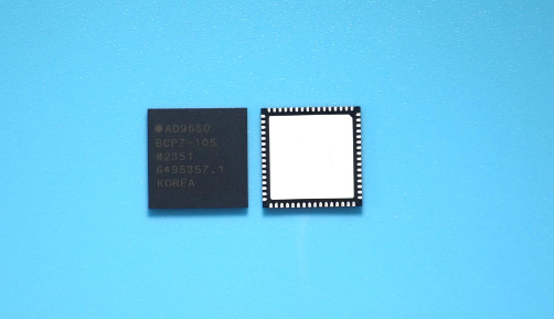
AD9650BCPZ-105 COUNTRY OF ORIGIN
|
AD9650BCPZ-105 PARAMETRIC INFO
|
AD9650BCPZ-105 PACKAGE INFO
|
AD9650BCPZ-105 MANUFACTURING INFO
|
AD9650BCPZ-105 PACKAGING INFO
|
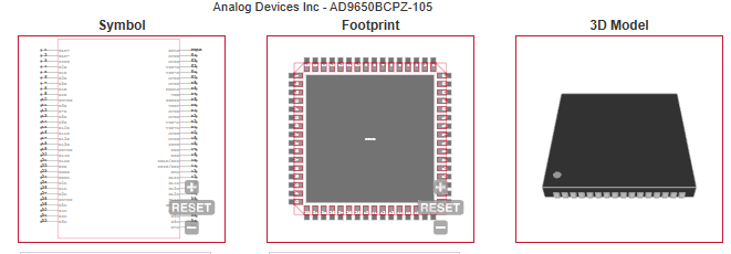
AD9650BCPZ-105 ECAD MODELS
|
AD9650BCPZ-105 APPLICATIONS
|
|
COUNTRY OF ORIGIN
|
Korea (Republic of)
|
Singapore
|
|
PARAMETRIC INFO
|
| Converter Type |
General Purpose |
| Input Type |
Voltage |
| Architecture |
Pipelined |
| Resolution |
16bit |
| Number of ADCs |
2 |
| Sampling Rate |
105Msps |
| Output Code |
2's Complement|Offset Binary |
| Maximum Analog Input Voltage |
2.2V |
| Minimum Analog Input Voltage |
-0.3V |
| Multiplying Function |
Yes |
| Digital Interface Type |
Parallel |
| Voltage Reference |
Internal|External |
| Minimum Positive Supply Voltage (V) |
1.7 |
| Input Signal Type |
Differential |
| Maximum Positive Supply Voltage (V) |
1.9 |
| Minimum Operating Temperature (°C) |
-40 |
| Maximum Operating Temperature (°C) |
85 |
| Supplier Temperature Grade |
Industrial |
| Minimum Storage Temperature (°C) |
-65 |
| Maximum Storage Temperature (°C) |
150 |
| Integral Nonlinearity Error |
±6LSB |
| Signal to Noise Ratio |
82.5dBFS(Typ) |
| Sample and Hold |
Yes |
| Number of Input Channels |
2 |
| Single-Ended Input |
No |
| Differential Input |
Yes |
| Input Voltage |
2.7Vp-p |
| Maximum Supply Current (mA) |
340 |
| Full Scale Error |
±2.5%FSR |
| Differential Nonlinearity |
-1/1.3LSB |
| Voltage Supply Source |
Single |
| Minimum Single Supply Voltage (V) |
1.7 |
| Typical Single Supply Voltage (V) |
1.8 |
| Maximum Single Supply Voltage (V) |
1.9 |
| Digital Supply Support |
No |
| Typical Power Dissipation (mW) |
663 |
| Parallel Interface |
Parallel CMOS|Parallel LVDS |
|
|
PACKAGE INFO
|
| Supplier Package |
LFCSP EP |
| Basic Package Type |
Non-Lead-Frame SMT |
| Pin Count |
64 |
| Lead Shape |
No Lead |
| PCB |
64 |
| Tab |
N/R |
| Pin Pitch (mm) |
0.5 |
| Package Length (mm) |
9 |
| Package Width (mm) |
9 |
| Package Height (mm) |
0.83 |
| Package Diameter (mm) |
N/R |
| Package Overall Length (mm) |
9 |
| Package Overall Width (mm) |
9 |
| Package Overall Height (mm) |
0.85 |
| Seated Plane Height (mm) |
0.85 |
| Mounting |
Surface Mount |
| Package Weight (g) |
N/A |
| Package Material |
Plastic |
| Package Description |
Lead Frame Chip Scale Package, Exposed Pad |
| Package Family Name |
CSP |
| Jedec |
MO-220VMMD-4 |
| Package Outline |
Link to Datasheet |
|
|
MANUFACTURING INFO
|
| MSL |
3 |
| Maximum Reflow Temperature (°C) |
260 |
| Reflow Solder Time (Sec) |
30 |
| Number of Reflow Cycle |
3 |
| Standard |
J-STD-020D |
| Maximum Wave Temperature (°C) |
N/R |
| Wave Solder Time (Sec) |
N/R |
| Wave Temp. Source |
Link to Datasheet |
| Lead Finish(Plating) |
Matte Sn annealed |
| Under Plating Material |
Ag |
| Terminal Base Material |
Cu Alloy |
| Number of Wave Cycles |
N/R |
|
|
PACKAGING INFO
|
| Packaging |
Tray |
| Quantity Of Packaging |
260 |
| Packaging Document |
Link to Datasheet |
|
|
ECAD MODELS
|
|
| |
| APPLICATIONS |
| • Industrial instrumentation
|
| • X-Ray, MRI, and ultrasound equipment |
| • High speed pulse acquisition |
| • Chemical and spectrum analysis |
| • Direct conversion receivers |
| • Multimode digitalreceivers |
| • Smart antenna systems |
| •General-purpose software radios |
| |