|
|
• Direct RF synthesis at 2.5 GSPS update rate DC to 1.25 GHz in baseband mode 1.25 GHz to 3.0 GHz in mix mode
|
• Industry leading single/multicarrier IF or RF synthesis fOUT = 350 MHz, ACLR =80 dBc fOUT = 950 MHz, ACLR = 78 dBc fOUT = 2100 MHz, ACLR = 69 dBc
|
• Dual-port LVDS data interface Up to 1.25 GSPS operation Source synchronous DDR clocking
|
• Pin-compatible with the AD9739A
|
• Multichip synchronization capability
|
• Programmable output current: 8.7 mA to 31.7 mA
|
• Low power: 1.16 W at 2.5 GSPS
|
|
| CATALOG |
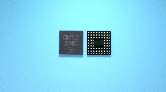
AD9739BBCZ COUNTRY OF ORIGIN
|
AD9739BBCZ PARAMETRIC INFO
|
AD9739BBCZ PACKAGE INFO
|
AD9739BBCZ MANUFACTURING INFO
|
AD9739BBCZ PACKAGING INFO
|
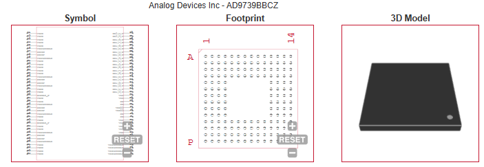
AD9739BBCZ ECAD MODELS
|
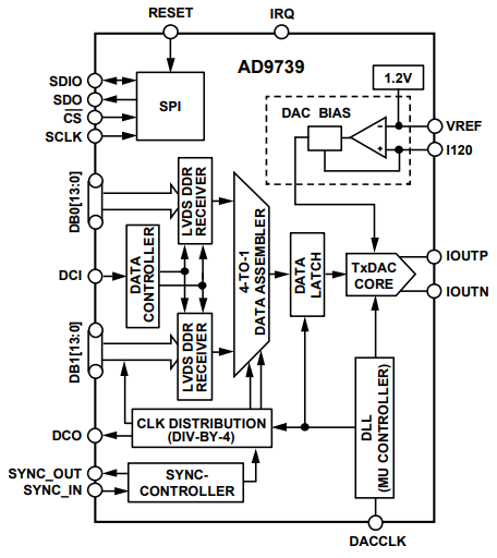
AD9739BBCZ FUNCTIONAL BLOCK DIAGRAM
|
AD9739BBCZ APPLICATIONS
|
|
COUNTRY OF ORIGIN
|
Korea (Republic of)
|
|
PARAMETRIC INFO
|
| Architecture |
Quad-Switch |
| Resolution |
14bit |
| Number of DAC Channels |
1 |
| Number of Outputs per Chip |
1 |
| Conversion Rate |
2.5Gsps |
| Converter Type |
RF |
| Output Type |
Current |
| Voltage Reference |
Internal|External |
| Maximum Settling Time (us) |
0.013(Typ) |
| Digital Interface Type |
LVDS |
| Output Polarity |
Unipolar |
| Integral Nonlinearity Error |
±1.3LSB(Typ) |
| Full Scale Error |
5.5%FSR(Typ) |
| Minimum Operating Temperature (°C) |
-40 |
| Maximum Operating Temperature (°C) |
85 |
| Minimum Storage Temperature (°C) |
-65 |
| Maximum Storage Temperature (°C) |
150 |
| Power Supply Type |
Analog and Digital |
| Minimum Single Supply Voltage (V) |
3.1 |
| Typical Single Supply Voltage (V) |
3.3 |
| Maximum Single Supply Voltage (V) |
3.5 |
| Digital Supply Support |
Yes |
| Maximum Power Dissipation (mW) |
975 |
|
|
PACKAGE INFO
|
| Supplier Package |
CSP-BGA |
| Basic Package Type |
Ball Grid Array |
| Pin Count |
160 |
| Lead Shape |
Ball |
| PCB |
160 |
| Tab |
N/R |
| Pin Pitch (mm) |
0.8 |
| Package Length (mm) |
12 |
| Package Width (mm) |
12 |
| Package Height (mm) |
1(Max) |
| Package Diameter (mm) |
N/R |
| Seated Plane Height (mm) |
1.4(Max) |
| Mounting |
Surface Mount |
| Package Weight (g) |
N/A |
| Package Material |
Plastic |
| Package Description |
Chip Scale Ball Grid Array Package |
| Package Family Name |
BGA |
| Jedec |
MO-205AE |
| Package Outline |
Link to Datasheet |
|
|
MANUFACTURING INFO
|
| MSL |
3 |
| Maximum Reflow Temperature (°C) |
260 |
| Reflow Solder Time (Sec) |
30 |
| Number of Reflow Cycle |
3 |
| Standard |
J-STD-020D |
| Maximum Wave Temperature (°C) |
N/R |
| Wave Solder Time (Sec) |
N/R |
| Lead Finish(Plating) |
SnAgCu |
| Under Plating Material |
N/A |
| Terminal Base Material |
N/A |
| Number of Wave Cycles |
N/R |
|
|
PACKAGING INFO
|
| Packaging |
Tray |
| Quantity Of Packaging |
189 |
| Packaging Document |
Link to Datasheet |
|
|
| ECAD MODELS |
 |
|
| FUNCTIONAL BLOCK DIAGRAM |
 |
|
| APPLICATIONS |
| • Broadband communications systems |
| • Military jammers |
| • Instrumentation, automatic test equipment |
| • Radar, avionics |
| |