 |
|
► Offset voltage:
► 25 µV maximum at 25°C (B grade, 8-lead SOIC, single/ dual)
► 50 µV maximum at 25°C (A grade, 8-lead SOIC, single/ dual)
► 50 µV maximum at 25°C (A grade, 14-lead SOIC, quad)
|
► Offset voltage drift:
► 0.25 µV/°C maximum (B grade, 8-lead SOIC, single/dual)
► 0.55 µV/°C maximum (A grade, 8-lead SOIC, single/dual)
► 0.75 µV/°C maximum (A grade, 14-lead SOIC, quad) |
| ► MSL1 rated |
| ► Low input bias current: 1 nA maximum at TA = 25°C
|
| ► Low voltage noise density: 6.9 nV/√Hz typical at f = 1000 Hz |
| ► CMRR, PSRR, and AV > 120 dB minimum |
| ► Low supply current: 400 µA per amplifier typical |
| ► Wide gain bandwidth product: 3.9 MHz at ±5 V |
► Dual-supply operation:
► Specified at ±5 V to ±15 V
► Operates at ±2.5 V to ±15 V |
| ► Unity gain stable |
| ► No phase reversal
|
| ► Long-term offset voltage drift (10,000 hours): 0.5 µV typical
|
| ► Temperature hysteresis: 1 µV typical |
|
| CATALOG |
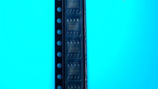
| ADA4077-2BRZ-R7 COUNTRY OF ORIGIN |
| ADA4077-2BRZ-R7 PARAMETRIC INFO |
| ADA4077-2BRZ-R7 PACKAGE INFO |
| ADA4077-2BRZ-R7 MANUFACTURING INFO |
| ADA4077-2BRZ-R7 PACKAGING INFO |
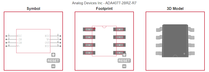
| ADA4077-2BRZ-R7 ECAD MODELS |
| ADA4077-2BRZ-R7 APPLICATIONS |
|
| COUNTRY OF ORIGIN |
| Ireland |
| Philippines |
|
| PARAMETRIC INFO |
| Manufacturer Type |
Precision Amplifier |
| Type |
Precision Amplifier |
| Number of Channels per Chip |
2 |
| Minimum PSRR (dB) |
123 |
| Minimum Dual Supply Voltage (V) |
±2.5 |
| Typical Gain Bandwidth Product (MHz) |
3.9 |
| Maximum Input Offset Voltage (mV) |
0.05@±5V |
| Typical Dual Supply Voltage (V) |
±3|±5|±9|±12 |
| Maximum Input Offset Current (uA) |
0.0005@±5V |
| Maximum Dual Supply Voltage (V) |
±15 |
| Maximum Operating Supply Voltage (V) |
±15 |
| Maximum Input Bias Current (uA) |
0.001@±5V |
| Minimum CMRR (dB) |
122 |
| Maximum Supply Voltage Range (V) |
30 to 32 |
| Minimum CMRR Range (dB) |
>=115 |
| Typical Voltage Gain (dB) |
130 |
| Typical Slew Rate (V/us) |
1.2@±5V |
| Typical Settling Time (ns) |
3000 |
| Typical Output Current (mA) |
10@±5V |
| Typical Input Noise Voltage Density (nV/rtHz) |
13@±5V |
| Typical Noninverting Input Current Noise Density (pA/rtHz) |
0.2@±5V |
| Shut Down Support |
No |
| Minimum Operating Temperature (°C) |
-40 |
| Maximum Operating Temperature (°C) |
125 |
| Supplier Temperature Grade |
Extended Industrial |
| Minimum Storage Temperature (°C) |
-65 |
| Maximum Storage Temperature (°C) |
150 |
| Power Supply Type |
Dual |
| Maximum Supply Current (mA) |
0.9@±15V |
|
| PACKAGE INFO |
| Supplier Package |
SOIC N |
| Basic Package Type |
Lead-Frame SMT |
| Pin Count |
8 |
| Lead Shape |
Gull-wing |
| PCB |
8 |
| Tab |
N/R |
| Pin Pitch (mm) |
1.27 |
| Package Length (mm) |
5(Max) |
| Package Width (mm) |
4(Max) |
| Package Height (mm) |
1.5(Max) |
| Package Diameter (mm) |
N/R |
| Package Overall Length (mm) |
5(Max) |
| Package Overall Width (mm) |
6.2(Max) |
| Package Overall Height (mm) |
1.75(Max) |
| Seated Plane Height (mm) |
1.75(Max) |
| Mounting |
Surface Mount |
| Package Weight (g) |
N/A |
| Package Material |
Plastic |
| Package Description |
Small Outline IC Narrow Body |
| Package Family Name |
SO |
| Jedec |
MS-012AA |
| Package Outline |
Link to Datasheet |
|
| MANUFACTURING INFO |
| MSL |
1 |
| Maximum Reflow Temperature (°C) |
260 |
| Reflow Solder Time (Sec) |
30 |
| Number of Reflow Cycle |
3 |
| Standard |
J-STD-020D |
| Maximum Wave Temperature (°C) |
300 |
| Wave Solder Time (Sec) |
10 |
| Wave Temp. Source |
Link to Datasheet |
| Lead Finish(Plating) |
Matte Sn annealed |
| Under Plating Material |
Ag |
| Terminal Base Material |
Cu Alloy |
|
| PACKAGING INFO |
| Packaging Suffix |
R7 |
| Packaging |
Tape and Reel |
| Quantity Of Packaging |
1000 |
| Reel Diameter (in) |
7 |
| Tape Pitch (mm) |
8 |
| Tape Width (mm) |
12 |
| Component Orientation |
Q1 |
| Packaging Document |
Link to Datasheet |
| Tape Material |
Plastic |
| Tape Type |
Embossed |
|
| ECAD MODELS |
 |
|
| APPLICATIONS |
| ► Process control front-end amplifiers |
| ► Optical network control circuits |
| ► Instrumentation |
| ► Precision sensors and controls |
| ► Precision filters |
|