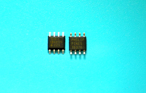
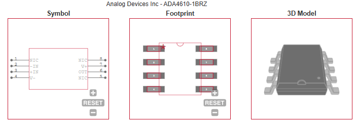
ADA4610-1BRZ Analog Devices IC OPAMP JFET RRO 8SOIC

label:
2024/08/7 168
ADA4610-1BRZ Analog Devices IC OPAMP JFET RRO 8SOIC


• Low offset voltage B grade: 0.4 mV maximum (ADA4610-1/ADA4610-2 only) A grade: 1 mV maximum
• Low input bias current: 5 pA typical
• Dual-supply operation: ±5 V to ±15 V
• Low voltage noise: 0.45 µV p-p at 0.1 Hz to 10 Hz
• Voltage noise density: 7.30 nV/√Hz at f = 1 kHz
• Low THD + N: 0.00025%


CATALOG
ADA4610-1BRZ COUNTRY OF ORIGIN
ADA4610-1BRZ PARAMETRIC INFO
ADA4610-1BRZ PACKAGE INFO
ADA4610-1BRZ MANUFACTURING INFO
ADA4610-1BRZ PACKAGING INFO
ADA4610-1BRZ ECAD MODELS
ADA4610-1BRZ APPLICATIONS


COUNTRY OF ORIGIN
Ireland
Philippines
China


PARAMETRIC INFO
Manufacturer Type Precision Amplifier
Type Precision Amplifier
Rail to Rail Rail to Rail Output
Number of Channels per Chip 1
Process Technology iPolar®
Minimum PSRR (dB) 104
Typical Input Resistance (Ohm) 10T
Maximum Quiescent Current (mA) 1.7@±5V
Minimum Dual Supply Voltage (V) ±5
Typical Gain Bandwidth Product (MHz) 15.4
Maximum Input Offset Voltage (mV) 0.4@±5V
Typical Dual Supply Voltage (V) ±9|±12
Maximum Input Offset Current (uA) 0.00002@±5V
Maximum Dual Supply Voltage (V) ±15
Maximum Input Voltage Range (V) -2.5 to 2.5
Maximum Operating Supply Voltage (V) ±15
Maximum Input Bias Current (uA) 0.000025@±5V
Minimum CMRR (dB) 94
Maximum Supply Voltage Range (V) 30 to 32
Minimum CMRR Range (dB) 90 to 95
Typical Voltage Gain (dB) 98
Typical Slew Rate (V/us) 46@±5V
Typical Input Offset Current (uA) 0.000002@±5V
Minimum Slew Rate (V/us) 15@±5V
Typical Input Noise Voltage Density (nV/rtHz) 14@±5V
Typical Input Bias Current (uA) 0.000005@±5V
Shut Down Support No
Minimum Operating Temperature (°C) -40
Maximum Operating Temperature (°C) 125
Supplier Temperature Grade Extended Industrial
Minimum Storage Temperature (°C) -65
Maximum Storage Temperature (°C) 150
Power Supply Type Dual
Typical High Level Output Voltage (V) 4.9
Typical Low Level Output Voltage (V) -4.95
Input Offset Voltage Drift (uV/°C) 2


PACKAGE INFO
Supplier Package SOIC N
Basic Package Type Lead-Frame SMT
Pin Count 8
Lead Shape Gull-wing
PCB 8
Tab N/R
Pin Pitch (mm) 1.27
Package Length (mm) 5(Max)
Package Width (mm) 4(Max)
Package Height (mm) 1.5(Max)
Package Diameter (mm) N/R
Package Overall Length (mm) 5(Max)
Package Overall Width (mm) 6.2(Max)
Package Overall Height (mm) 1.75(Max)
Seated Plane Height (mm) 1.75(Max)
Mounting Surface Mount
Package Weight (g) N/A
Package Material Plastic
Package Description Small Outline IC Narrow Body
Package Family Name SO
Jedec MS-012AA
Package Outline Link to Datasheet


MANUFACTURING INFO
MSL 1
Maximum Reflow Temperature (°C) 260
Reflow Solder Time (Sec) 30
Number of Reflow Cycle 3
Standard J-STD-020D
Maximum Wave Temperature (°C) N/R
Wave Solder Time (Sec) N/R
Wave Temp. Source Link to Datasheet
Lead Finish(Plating) Matte Sn annealed
Under Plating Material Ag
Terminal Base Material Cu Alloy
Number of Wave Cycles N/R


PACKAGING INFO
Packaging Tube
Quantity Of Packaging 98
Packaging Document Link to Datasheet


ECAD MODELS


APPLICATIONS
• Instrumentation
• Medical instruments
• Multipole filters
• Precision current measurement
• Photodiode amplifiers
• Sensors
• Audio
Продукт RFQ