|
| |
• Small signal bandwidth: 260 MHz
|
• Ultralow power 1.25mA
|
• Extremely low harmonic distortion−122 dB THD at 50 kHz−96 dB THD at 1 MHz
|
| • Low input voltage noise: 3.9 nV/√Hz |
| • 0.35 mV maximum offset voltage |
| • Balanced outputs |
| • Settling time to 0.1%: 34 ns |
| • Rail-to-rail output: −VS + 0.1 V to +VS − 0.1 V |
| • Adjustable output common-mode voltage |
| • Flexible power supplies: 3 V to 7 V (LFCSP) |
| • Disable pin to reduce power consumption |
| |
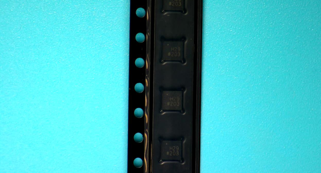
| CATALOG |
| ADA4940-1ACPZ-R7 COUNTRY OF ORIGIN |
ADA4940-1ACPZ-R7 PARAMETRIC INFO
|
ADA4940-1ACPZ-R7 PACKAGE INFO
|
ADA4940-1ACPZ-R7 MANUFACTURING INFO
|
ADA4940-1ACPZ-R7 PACKAGING INFO
|
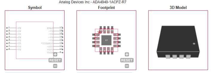
ADA4940-1ACPZ-R7 EACD MODELS
|
| ADA4940-1ACPZ-R7 APPLICATIONS |
|
| COUNTRY OF ORIGIN |
| United States of America |
| Malaysia |
| Philippines |
|
PARAMETRIC INFO
|
| Type |
Differential Amplifier |
| Rail to Rail |
Rail to Rail Output |
| Number of Elements per Chip |
1 |
| Number of Channels per Chip |
1 |
| Output Type |
Differential |
| Minimum PSRR (dB) |
80 |
| Maximum Input Offset Voltage (mV) |
0.35@5V |
| Maximum Input Bias Current (uA) |
1.6(Min)@5V |
| Minimum CMRR (dB) |
86 |
| Process Technology |
SiGe |
| Minimum CMRR Range (dB) |
85 to 95 |
| Maximum Quiescent Current (mA) |
1.38@5V |
| Output Logic Level |
CML |
| Typical Output Current (mA) |
46@5V |
| Maximum Input Resistance (MOhm) |
50(Typ)@5V |
| Typical Slew Rate (V/us) |
95@5V |
| Typical Input Offset Current (uA) |
0.05@5V |
| Maximum Input Offset Current (uA) |
0.5@5V |
| Maximum Voltage Gain Range (dB) |
75 to 100 |
| Maximum Voltage Gain (dB) |
99(Typ) |
| Minimum Operating Temperature (°C) |
-40 |
| Maximum Operating Temperature (°C) |
125 |
| Minimum Storage Temperature (°C) |
-65 |
| Maximum Storage Temperature (°C) |
150 |
| Power Supply Type |
Single |
| Maximum Supply Voltage Range (V) |
7 to 10 |
| Minimum Single Supply Voltage (V) |
3 |
| Typical Single Supply Voltage (V) |
5 |
| Maximum Single Supply Voltage (V) |
7 |
| Maximum Operating Supply Voltage (V) |
7 |
|
|
PACKAGE INFO
|
| Supplier Package |
LFCSP EP |
| Basic Package Type |
Non-Lead-Frame SMT |
| Pin Count |
16 |
| Lead Shape |
No Lead |
| PCB |
16 |
| Tab |
N/R |
| Pin Pitch (mm) |
0.5 |
| Package Length (mm) |
3 |
| Package Width (mm) |
3 |
| Package Height (mm) |
0.73 |
| Package Diameter (mm) |
N/R |
| Package Overall Length (mm) |
3 |
| Package Overall Width (mm) |
3 |
| Package Overall Height (mm) |
0.75 |
| Seated Plane Height (mm) |
0.75 |
| Mounting |
Surface Mount |
| Package Weight (g) |
N/A |
| Package Material |
Plastic |
| Package Description |
Lead Frame Chip Scale Package, Exposed Pad |
| Package Family Name |
CSP |
| Jedec |
MO-220WEED-6 |
| Package Outline |
Link to Datasheet |
|
|
MANUFACTURING INFO
|
| MSL |
3 |
| Maximum Reflow Temperature (°C) |
260 |
| Reflow Solder Time (Sec) |
30 |
| Number of Reflow Cycle |
3 |
| Standard |
J-STD-020D |
| Maximum Wave Temperature (°C) |
N/R |
| Wave Solder Time (Sec) |
N/R |
| Lead Finish(Plating) |
Matte Sn annealed |
| Under Plating Material |
Ag |
| Terminal Base Material |
Cu Alloy |
| Number of Wave Cycles |
N/R |
|
|
PACKAGING INFO
|
| Packaging Suffix |
R7 |
| Packaging |
Tape and Reel |
| Quantity Of Packaging |
1500 |
| Reel Diameter (in) |
7 |
| Tape Pitch (mm) |
8 |
| Tape Width (mm) |
12 |
| Component Orientation |
Q2 |
| Packaging Document |
Link to Datasheet |
| Tape Material |
Plastic |
| Tape Type |
Embossed |
|
|
ECAD MODELS
|
|
|
| APPLICATIONS |
| • Low power PulSAR®/SAR ADC drivers
|
| • Single-ended-to-differential conversion |
| • Differential buffers |
• Line drivers
|
| • Medical imaging |
| • Industrial process controls |
| • Portable electronics |
| |