 |
|
| • Eight Input Channels |
| • Variable Power Management |
| • Independent Analog and Digital Supplies |
| • SPI/QSPI™ /MICROWIRE™/DSP Compatible
|
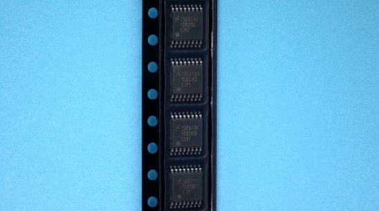
| • Packaged in 16-Lead TSSOP |
• Key Specifications
– Conversion Rate 500 ksps to 1 MSPS
– DNL (VA = VD = 5.0 V) +1.5 / −0.9
– LSB (maximum) INLL (VA = VD = 5.0 V) ±1.2 LSB (maximum)
– Power Consumption
– 3V Supply 2.3 mW (typical)
– 5V Supply 10.7 mW (typical)
|
|
| CATALOG |
| ADC128S102CIMTX/NOPB COUNTRY OF ORIGIN |
| ADC128S102CIMTX/NOPB PARAMETRIC INFO |
| ADC128S102CIMTX/NOPB PACKAGE INFO |
| ADC128S102CIMTX/NOPB MANUFACTURING INFO |
| ADC128S102CIMTX/NOPB PACKAGING INFO |
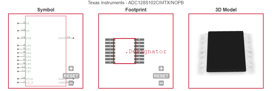
| ADC128S102CIMTX/NOPB ECAD MODELS |
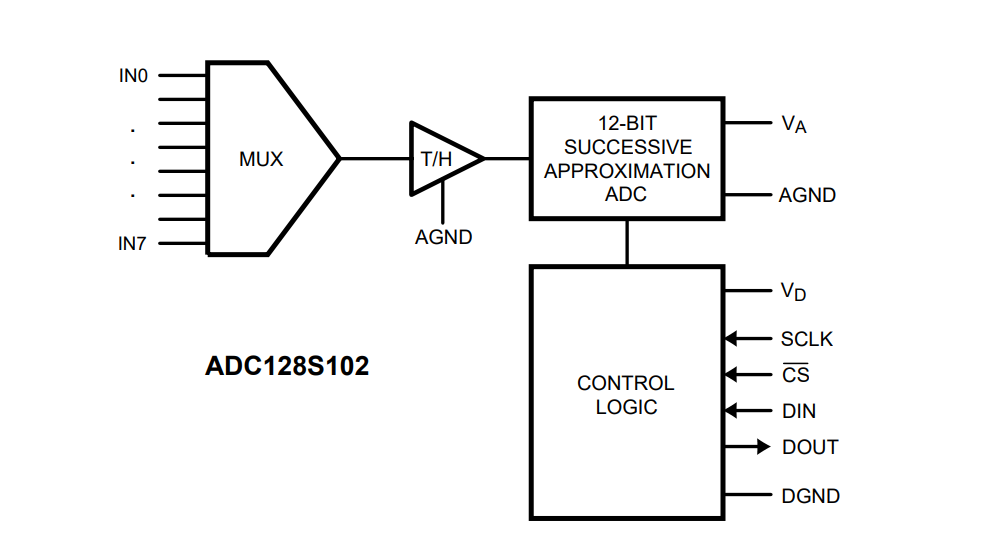
| ADC128S102CIMTX/NOPB FUNCTIONAL BLOCK DIAGRAM |
| ADC128S102CIMTX/NOPB APPLICATIONS |
|
| COUNTRY OF ORIGIN |
| China |
| Malaysia |
|
| PARAMETRIC INFO |
| Converter Type |
General Purpose |
| Input Type |
Voltage |
| Architecture |
SAR |
| Resolution |
12bit |
| Number of ADCs |
1 |
| Sampling Rate |
1Msps |
| Digital Interface Type |
Serial (SPI, QSPI, Microwire) |
| Voltage Reference |
Supply |
| Minimum Positive Supply Voltage (V) |
2.7 |
| Maximum Positive Supply Voltage (V) |
5.25 |
| Input Signal Type |
Single-Ended |
| Process Technology |
CMOS |
| Polarity of Input Voltage |
Unipolar |
| Minimum Operating Temperature (°C) |
-40 |
| Maximum Operating Temperature (°C) |
105 |
| Supplier Temperature Grade |
Extended Industrial |
| Integral Nonlinearity Error |
±1.2LSB |
| Signal to Noise Ratio |
73dB(Typ) |
| Sample and Hold |
Yes |
| Number of Input Channels |
8 |
| Single-Ended Input |
Yes |
| Differential Input |
No |
| Input Voltage |
5.25V |
| No Missing Codes (bit) |
12 |
| Full Scale Error |
±2LSB |
| Differential Nonlinearity |
-0.9/1.5LSB |
| Voltage Supply Source |
Single |
| Minimum Single Supply Voltage (V) |
2.7 |
| Typical Single Supply Voltage (V) |
3.3|5 |
| Maximum Single Supply Voltage (V) |
5.25 |
| Digital Supply Support |
No |
| Maximum Power Dissipation (mW) |
1200 |
|
| |
| PACKAGE INFO |
| Supplier Package |
TSSOP |
| Basic Package Type |
Lead-Frame SMT |
| Pin Count |
16 |
| Lead Shape |
Gull-wing |
| PCB |
16 |
| Tab |
N/R |
| Pin Pitch (mm) |
0.65 |
| Package Length (mm) |
5.1(Max) |
| Package Width (mm) |
4.5(Max) |
| Package Height (mm) |
1.05(Max) |
| Package Diameter (mm) |
N/R |
| Package Overall Length (mm) |
5.1(Max) |
| Package Overall Width (mm) |
6.6(Max) |
| Package Overall Height (mm) |
1.2(Max) |
| Seated Plane Height (mm) |
1.2(Max) |
| Mounting |
Surface Mount |
| Package Weight (g) |
N/A |
| Package Material |
Plastic |
| Package Description |
Thin Shrink Small Outline Package |
| Package Family Name |
SO |
| Jedec |
MO-153AB |
| Package Outline |
Link to Datasheet |
|
| |
| MANUFACTURING INFO |
| MSL |
1 |
| Maximum Reflow Temperature (°C) |
260 |
| Reflow Solder Time (Sec) |
30 |
| Number of Reflow Cycle |
3 |
| Standard |
J-STD-020D |
| Reflow Temp. Source |
Link to Datasheet |
| Maximum Wave Temperature (°C) |
N/R |
| Wave Solder Time (Sec) |
N/R |
| Lead Finish(Plating) |
Matte Sn |
| Under Plating Material |
N/A |
| Terminal Base Material |
Cu Alloy |
|
| |
| PACKAGING INFO |
| Packaging Suffix |
X |
| Packaging |
Tape and Reel |
| Quantity Of Packaging |
2500 |
|
| |
| ECAD MODELS |
 |
|
| FUNCTIONAL BLOCK DIAGRAM |
 |
|
| APPLICATIONS |
| • Automotive Navigation |
| • Portable Systems |
| • Medical Instruments |
| • Mobile Communications |
| • Instrumentation and Control Systems |
|