
|
|
• Fully specified rail to rail at VCC = 2.5 V to 5.5 V
|
• Input common-mode voltage from −0.2 V to VCC + 0.2 V
|
• Low glitch CMOS-/TTL-compatible output stage
|
• 3.5 ns propagation delay
|
• 10 mW at 3.3 V
|
• Shutdown pin
|
• Single-pin control for programmable hysteresis and latch
|
• Power supply rejection > 50 dB
|
• Improved replacement for MAX999
|
• −40°C to +125°C operation
|
|
| CATALOG |
ADCMP600BKSZ-REEL7 COUNTRY OF ORIGIN
|
ADCMP600BKSZ-REEL7 PARAMETRIC INFO
|
ADCMP600BKSZ-REEL7 PACKAGE INFO
|
ADCMP600BKSZ-REEL7 MANUFACTURING INFO
|
ADCMP600BKSZ-REEL7 PACKAGING INFO
|
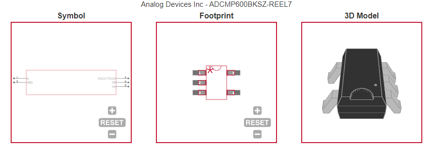
ADCMP600BKSZ-REEL7 ECAD MODELS
|
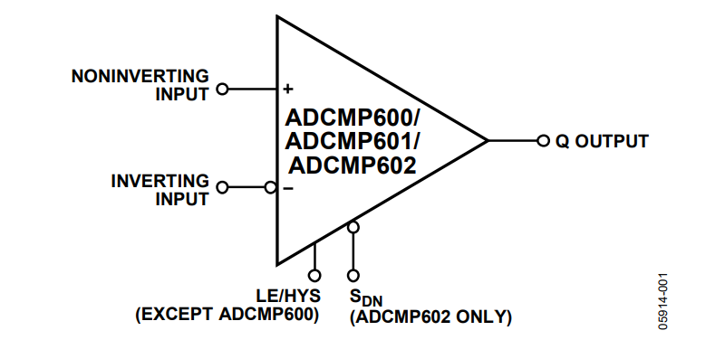
ADCMP600BKSZ-REEL7 FUNCTIONAL BLOCK DIAGRAM
|
ADCMP600BKSZ-REEL7 APPLICATIONS
|
|
COUNTRY OF ORIGIN
|
Malaysia
|
|
PARAMETRIC INFO
|
| Rail to Rail |
Rail to Rail Input/Output |
| Manufacturer Type |
High Speed Comparator |
| Process Technology |
XFCB2 |
| Number of Channels per Chip |
1 |
| Typical PSRR (dB) |
50(Min) |
| Output Type |
CMOS/TTL |
| Maximum Input Offset Voltage (mV) |
5@2.5V |
| Maximum Input Bias Current (uA) |
5@2.5V |
| Typical CMRR (dB) |
50(Min) |
| Typical Voltage Gain (dB) |
85 |
| Typical Voltage Gain Range (dB) |
70 to 90 |
| Strobe Capability |
No |
| Typical Output Current (mA) |
50(Max) |
| Maximum Input Offset Current (uA) |
2@2.5V |
| Maximum Propagation Delay Time (ns) |
5(Typ) |
| Minimum Operating Temperature (°C) |
-40 |
| Maximum Operating Temperature (°C) |
125 |
| Minimum Storage Temperature (°C) |
-65 |
| Maximum Storage Temperature (°C) |
150 |
| Power Supply Type |
Single |
| Integrated Voltage Reference |
No |
| Maximum Test Temperature (°C) |
125 |
| Minimum Test Temperature (°C) |
-40 |
| Maximum Operating Supply Voltage (V) |
5.5 |
| Integrated OP Amp |
No |
| Minimum Single Supply Voltage (V) |
2.5 |
| Typical Single Supply Voltage (V) |
3|5 |
| Maximum Single Supply Voltage (V) |
5.5 |
| Maximum Supply Current (mA) |
4@5.5V |
|
|
PACKAGE INFO
|
| Supplier Package |
SC-70 |
| Basic Package Type |
Lead-Frame SMT |
| Pin Count |
5 |
| Lead Shape |
Gull-wing |
| PCB |
5 |
| Tab |
N/R |
| Pin Pitch (mm) |
0.65 |
| Package Length (mm) |
2 |
| Package Width (mm) |
1.25 |
| Package Height (mm) |
0.9 |
| Package Diameter (mm) |
N/R |
| Seated Plane Height (mm) |
1.1(Max) |
| Mounting |
Surface Mount |
| Package Weight (g) |
N/A |
| Package Material |
Plastic |
| Package Description |
Small Outline Transistor |
| Package Family Name |
SOT |
| Jedec |
MO-203AA |
| Package Outline |
Link to Datasheet |
|
|
MANUFACTURING INFO
|
| MSL |
1 |
| Maximum Reflow Temperature (°C) |
260 |
| Reflow Solder Time (Sec) |
30 |
| Number of Reflow Cycle |
3 |
| Standard |
J-STD-020D |
| Maximum Wave Temperature (°C) |
N/R |
| Wave Solder Time (Sec) |
N/R |
| Wave Temp. Source |
Link to Datasheet |
| Lead Finish(Plating) |
Au |
| Under Plating Material |
Pd over Ni |
| Terminal Base Material |
Cu Alloy |
| Number of Wave Cycles |
N/R |
|
|
PACKAGING INFO
|
| Packaging Suffix |
REEL7 |
| Packaging |
Tape and Reel |
| Quantity Of Packaging |
3000 |
| Reel Diameter (in) |
7 |
| Packaging Document |
Link to Datasheet |
|
|
ECAD MODELS
|
|
|
FUNCTIONAL BLOCK DIAGRAM
|
|
|
APPLICATIONS
|
• High speed instrumentation
|
• Clock and data signal restoration
|
• Logic level shifting or translation
|
• Pulse spectroscopy
|
• High speed line receivers
|
• Threshold detection
|
• Peak and zero-crossing detectors
|
• High speed trigger circuitry
|
• Pulse-width modulators
|
• Current/voltage-controlled oscillators
|
| • Automatic test equipment (ATE) |
|