|
| |
• RF bandwidth to 13 GHz
|
• High and low speed FMCW ramp generation
|
• 25-bit fixed modulus allows subhertz frequency resolution
|
| • PFD frequencies up to 110 MHz |
| • Normalized phase noise floor of −224 dBc/Hz |
| • FSK and PSK functions |
| • Sawtooth, triangular, and parabolic waveform generation |
| • Ramp superimposed with FSK |
| • Ramp with 2 different sweep rates |
| • Ramp delay, frequency readback, and interrupt functions |
| • Programmable phase control |
| • 2.7 V to 3.45 V analog power supply |
| • 1.8 V digital power supply |
| • Programmable charge pump currents |
| • 3-wire serial interface |
| • Digital lock detect |
| • ESD performance: 3000 V HBM, 1000 V CDM |
| • Qualified for automotive applications |
| |
| CATALOG |
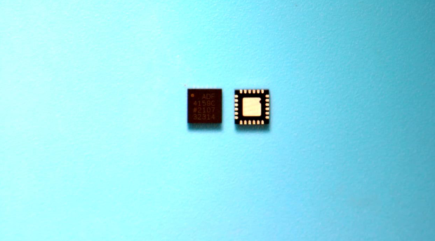
| ADF4159CCPZ-RL7 COUNTRY OF ORIGIN |
ADF4159CCPZ-RL7 PARAMETRIC INFO
|
ADF4159CCPZ-RL7 PACKAGE INFO
|
ADF4159CCPZ-RL7 MANUFACTURING INFO
|
ADF4159CCPZ-RL7 PACKAGING INFO
|
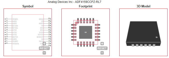
ADF4159CCPZ-RL7 EACD MODELS
|
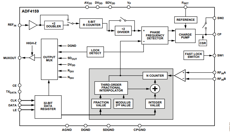
| ADF4159CCPZ-RL7 FUNCTIONAL BLOCK DIAGRAM |
| ADF4159CCPZ-RL7 APPLICATIONS |
|
| COUNTRY OF ORIGIN |
| Thailand |
| Korea (Republic of) |
| Philippines |
|
PARAMETRIC INFO
|
| Number of Outputs per Chip |
1 |
| Clock Input Frequency (MHz) |
500 to 13000 |
| Maximum Output Frequency (MHz) |
2000 |
| Input Logic Level |
CMOS|TTL |
| Minimum Operating Temperature (°C) |
-40 |
| Maximum Operating Temperature (°C) |
125 |
| Input Signal Type |
Differential |
| Output Signal Type |
Single-Ended |
| Hitless Protection Switching |
No |
| Frequency Margining |
No |
| Programmability |
Yes |
| Minimum Storage Temperature (°C) |
-65 |
| Maximum Storage Temperature (°C) |
125 |
| Minimum Operating Supply Voltage (V) |
2.7 |
| Typical Operating Supply Voltage (V) |
2.5|3.3 |
| Maximum Operating Supply Voltage (V) |
3.45 |
| Number of Clock Inputs |
2 |
| Spread Spectrum |
No |
| Maximum Supply Current (mA) |
40 |
|
|
PACKAGE INFO
|
| Supplier Package |
LFCSP EP |
| Basic Package Type |
Non-Lead-Frame SMT |
| Pin Count |
24 |
| Lead Shape |
No Lead |
| PCB |
24 |
| Tab |
N/R |
| Pin Pitch (mm) |
0.5 |
| Package Length (mm) |
4 |
| Package Width (mm) |
4 |
| Package Height (mm) |
0.73 |
| Package Diameter (mm) |
N/R |
| Package Overall Length (mm) |
4 |
| Package Overall Width (mm) |
4 |
| Package Overall Height (mm) |
0.75 |
| Seated Plane Height (mm) |
0.75 |
| Mounting |
Surface Mount |
| Package Weight (g) |
N/A |
| Package Material |
Plastic |
| Package Description |
Lead Frame Chip Scale Package, Exposed Pad |
| Package Family Name |
CSP |
| Jedec |
MO-220WGGD-8 |
| Package Outline |
Link to Datasheet |
|
|
MANUFACTURING INFO
|
| MSL |
3 |
| Maximum Reflow Temperature (°C) |
260 |
| Reflow Solder Time (Sec) |
30 |
| Number of Reflow Cycle |
3 |
| Standard |
J-STD-020D |
| Maximum Wave Temperature (°C) |
N/R |
| Wave Solder Time (Sec) |
N/R |
| Lead Finish(Plating) |
Matte Sn annealed |
| Under Plating Material |
Ag |
| Terminal Base Material |
Cu Alloy |
| Number of Wave Cycles |
N/R |
|
|
PACKAGING INFO
|
| Packaging Suffix |
RL7 |
| Packaging |
Tape and Reel |
| Quantity Of Packaging |
1500 |
| Reel Diameter (in) |
7 |
| Tape Pitch (mm) |
8 |
| Tape Width (mm) |
12 |
| Component Orientation |
Q2 |
| Packaging Document |
Link to Datasheet |
| Tape Material |
Plastic |
| Tape Type |
Embossed |
|
|
ECAD MODELS
|
|
|
| FUNCTIONAL BLOCK DIAGRAM |
 |
|
| APPLICATIONS |
| • FMCW radars |
| • Communications test equipment |
| • Communications infrastructure |
| |