ADG1208YRUZ-REEL7 Analog Devices IC MULTIPLEXER 8X1 16TSSOP

label:
2024/08/8 161
ADG1208YRUZ-REEL7 Analog Devices IC MULTIPLEXER 8X1 16TSSOP


• <1 pC charge injection over full signal range
• 1 pF off capacitance
• 33 V supply range
• 120 Ω on resistance
• Fully specified at ±15 V/+12 V
• 3 V logic compatible inputs
• Rail-to-rail operation
• Break-before-make switching action
• Available in a 16-lead TSSOP, a 16-lead LFCSP, and a 16-lead SOIC
• Typical power consumption < 0.03 µW


CATALOG
ADG1208YRUZ-REEL7 COUNTRY OF ORIGIN
ADG1208YRUZ-REEL7 PARAMETER INFORMATION
ADG1208YRUZ-REEL7 PACKAGING INFORMATION
ADG1208YRUZ-REEL7 MANUFACTURING INFORMATION
ADG1208YRUZ-REEL7 TYPE OF PACKAGING
ADG1208YRUZ-REEL7 ECAD MODELS
ADG1208YRUZ-REEL7 FUNCTIONAL BLOCK DIAGRAMS
ADG1208YRUZ-REEL7 APPLICATIONS


COUNTRY OF ORIGIN
Taiwan (Province of China)
Malaysia
Philippines


PARAMETER INFORMATION
type Analog Multiplexer
Number of Channels per Chip 1
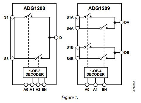
Multiplexer Architecture 8:1
Maximum On Resistance Range (Ohm) 400 to 1000
Configuration Single 8:1
Number of Inputs per Chip 8
Function General
Latch-Up Proof no
Typical Switch On Capacitance (pF) 9
Typical Switch Off Capacitance (pF) 7.5
Typical Off Leakage Current (nA) ±0.1
Typical Off Isolation (dB) -85
Typical Crosstalk (dB) -85
Maximum On Resistance Match Between Switches (Ohm) 6
Maximum On Resistance Flatness (Ohm) 64
Typical Charge Injection (pC) 0.4
Number of Outputs per Chip 1
Chip Enable Signals yes
Maximum On Resistance (Ohm) 475@12V/200@±15V
Maximum Propagation Delay Bus to Bus (ns) 130@±15V|170(Typ)@12V
Maximum Turn-On Time (ns) 95@±15V
Maximum Turn-Off Time (ns) 100@±15V
Input Signal Type Single
Output Signal Type Single
Propagation Delay Test Condition (pF) 35
Maximum High Level Output Current (mA) 30
Maximum Frequency (25°C) @ Vcc (MHz) 550(Typ)@±15V|450(Typ)@12V
Special Features Break-Before-Make
Minimum Operating Temperature (°C) -40
Maximum Operating Temperature (°C) 125
Vendor Temperature Grade Industrial
Maximum Storage Temperature (°C) 150
Minimum Storage Temperature (°C) -65
Power Supply Type Single|Dual
Minimum Single Supply Voltage (V) 5
Typical Single Supply Voltage (V) 12
Maximum Single Supply Voltage (V) 16.5
Minimum Dual Supply Voltage (V) ±5
Typical Dual Supply Voltage (V) ±15
Maximum Dual Supply Voltage (V) ±16.5
Typical Supply Current (mA) 0.22@16.5V/-0.000002@-16.5V
Maximum Supply Current (mA) 0.38@16.5V/-0.001@-16.5V@-40C to 125C


PACKAGING INFORMATION
Supplier Packaging TSSOP
Basic package types Lead-Frame SMT
Number of Pins 16
Pin shape Gull-wing
PCB 16
Ear piece N/R
Pin spacing (mm) 0.65
Package length (mm) 5
Package width (mm) 4.4
Package height (mm) 1.05(Max)
Package diameter (mm) N/R
Package Overall Length (mm) 5
Package Overall Width (mm) 6.4
Package Overall Height (mm) 1.2(Max)
Mounting surface height (mm) 1.2(Max)
Install Surface Mount
Package weight (g) not applicable
Packaging materials Plastic
package instruction Thin Shrink Small Outline Package
Package Series Name SO
JEDEC MO-153AB
Package Outline Link to data sheet


MANUFACTURING INFORMATION
MSL 1
Maximum reflow temperature (°C) 260
Reflow time (seconds) 30
Reflow cycles 3
standard J-STD-020D
Maximum wave soldering temperature (°C) N/R
Wave soldering time (seconds) N/R
Lead Finish(Plating) Matte Sn annealed
Plating materials Ag
Terminal base material Cu Alloy
Number of Wave Cycles N/R


TYPE OF PACKAGING
Packaging Suffix REEL7
Package Tape and Reel Packaging
Packing quantity 1000
Reel Diameter (in) 7
Tape Pitch (mm) 8
Tape Width (mm) 16
Component Orientation Q1
Package Type File Link to data sheet
Tape Material Plastic
Tape Type Embossed


ECAD MODELS


FUNCTIONAL BLOCK DIAGRAMS


APPLICATIONS
• Audio and video routing
• Automatic test equipment
• Data-acquisition systems
• Battery-powered systems
• Sample-and-hold systems
• Communication systems
Продукт RFQ