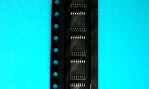
ADG451BRUZ-REEL7 Analog Devices IC SWITCH QUAD SPST 16TSSOP

label:
2024/01/11 257


• Low on resistance (4 Ω)  
• On resistance flatness (0.2 Ω)  
• 44 V supply maximum ratings  
• ±15 V analog signal range  
• Fully specified at ±5 V, 12 V, ±15 V  
• Ultralow power dissipation (18 μW)
• ESD 2 kV  
• Continuous current (100 mA)  
• Fast switching times
• tON 70 ns  
• tOFF 60 ns
• TTL-/CMOS-compatible   
• Pin-compatible upgrade for ADG411/ADG412/ADG413
   - and ADG431/ADG432/ADG433     


CATALOG
ADG451BRUZ-REEL7 COUNTRY OF ORIGIN
ADG451BRUZ-REEL7 PARAMETRIC INFO
ADG451BRUZ-REEL7 PACKAGE INFO
ADG451BRUZ-REEL7 MANUFACTURING INFO
ADG451BRUZ-REEL7 PACKAGING INFO
ADG451BRUZ-REEL7 ECAD MODELS
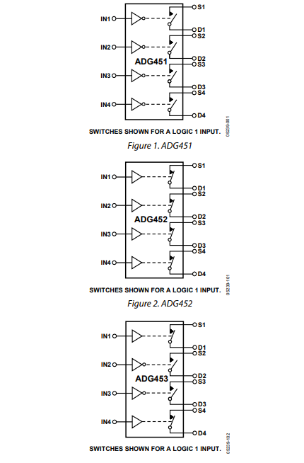
ADG451BRUZ-REEL7 FUNCTIONAL BLOCK DIAGRAMS  
ADG451BRUZ-REEL7 APPLICATIONS


COUNTRY OF ORIGIN
Taiwan (Province of China)
Philippines
Malaysia


PARAMETRIC INFO
Type Analog Switch
Number of Channels per Chip 4
Switch Architecture SPST
Polarity Non-Inverting
Maximum On Resistance Range (Ohm) 10 to 25
Configuration Quad SPST
Number of Inputs per Chip 4
Number of Outputs per Chip 4
Function General
Latch-Up Proof No
Typical Switch On Capacitance (pF) 148
Typical Switch Off Capacitance (pF) 60
Typical Off Leakage Current (nA) ±0.02
Typical Off Isolation (dB) 65
Typical Crosstalk (dB) -90
Maximum On Resistance Match Between Switches (Ohm) 0.5
Maximum On Resistance Flatness (Ohm) 1(Typ)
Typical Charge Injection (pC) 20
Chip Enable Signals Yes
Maximum On Resistance (Ohm) 12@±3.5V
Maximum Turn-On Time (ns) 220@12V
Maximum Turn-Off Time (ns) 160@12V
Maximum Power Dissipation (mW) 450
Input Signal Type Single
Output Signal Type Single
Maximum High Level Output Current (mA) 100
Switch Control Logic Active Low
Switch Normal Position NC
Minimum Operating Temperature (°C) -40
Maximum Operating Temperature (°C) 85
Supplier Temperature Grade Industrial
Maximum Storage Temperature (°C) 150
Minimum Storage Temperature (°C) -65
Power Supply Type Single|Dual
Minimum Single Supply Voltage (V) 5
Typical Single Supply Voltage (V) 9
Maximum Single Supply Voltage (V) 12
Minimum Dual Supply Voltage (V) ±4.5
Typical Dual Supply Voltage (V) ±5|±15
Maximum Dual Supply Voltage (V) ±20
Typical Supply Current (mA) ±0.0000001@±5V
Maximum Supply Current (mA) ±0.005@±5V@-40C to 85C


PACKAGE INFO
Supplier Package TSSOP
Basic Package Type Lead-Frame SMT
Pin Count 16
Lead Shape Gull-wing
PCB 16
Tab N/R
Pin Pitch (mm) 0.65
Package Length (mm) 5
Package Width (mm) 4.4
Package Height (mm) 1.05(Max)
Package Diameter (mm) N/R
Package Overall Length (mm) 5
Package Overall Width (mm) 6.4
Package Overall Height (mm) 1.2(Max)
Seated Plane Height (mm) 1.2(Max)
Mounting Surface Mount
Package Weight (g) N/A
Package Material Plastic
Package Description Thin Shrink Small Outline Package
Package Family Name SO
Jedec MO-153AB
Package Outline Link to Datasheet


MANUFACTURING INFO
MSL 1
Maximum Reflow Temperature (°C) 260
Reflow Solder Time (Sec) 30
Number of Reflow Cycle 3
Standard J-STD-020D
Maximum Wave Temperature (°C) N/R
Wave Solder Time (Sec) N/R
Lead Finish(Plating) Matte Sn annealed
Under Plating Material Ag
Terminal Base Material Cu Alloy
Number of Wave Cycles N/R


PACKAGING INFO
Packaging Suffix REEL7
Packaging Tape and Reel
Quantity Of Packaging 1000
Reel Diameter (in) 7
Tape Pitch (mm) 8
Tape Width (mm) 16
Component Orientation Q1
Packaging Document Link to Datasheet
Tape Material Plastic
Tape Type Embossed


ECAD MODELS


FUNCTIONAL BLOCK DIAGRAMS  


APPLICATIONS
• Relay replacement
• Audio and video switching
• Automatic test equipment
• Precision data acquisition
• Battery-powered systems  
• Sample-and-hold systems
• Communication systems  
• PBX, PABX systems  
• Avionics  


Продукт RFQ