| Type |
Analog Switch |
| Number of Channels per Chip |
1 |
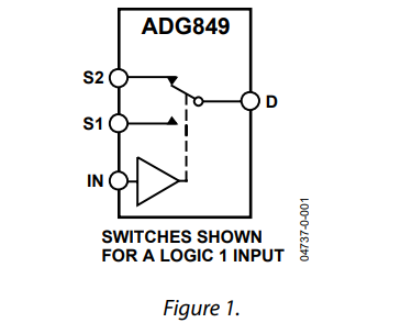
| Switch Architecture |
SPDT |
| Polarity |
Non-Inverting |
| Maximum On Resistance Range (Ohm) |
1 to 5 |
| Configuration |
Single SPDT |
| Number of Inputs per Chip |
1 |
| Process Technology |
CMOS |
| Number of Outputs per Chip |
2 |
| Function |
General |
| Latch-Up Proof |
No |
| Typical Off Leakage Current (nA) |
±0.04 |
| Typical Off Isolation (dB) |
-64 |
| Typical Crosstalk (dB) |
-64 |
| Maximum On Resistance Flatness (Ohm) |
0.24 |
| Typical Charge Injection (pC) |
30 |
| Chip Enable Signals |
Yes |
| Maximum On Resistance (Ohm) |
1.1@3.6V |
| Maximum Turn-On Time (ns) |
22@3.6V |
| Maximum Turn-Off Time (ns) |
18@3.6V |
| Input Signal Type |
Single |
| Output Signal Type |
Single |
| Maximum High Level Output Current (mA) |
400 |
| Maximum Frequency (25°C) @ Vcc (MHz) |
38(Typ)@5.5V |
| Special Features |
Break-Before-Make |
| Switch Control Logic |
Active Low/High |
| Switch Normal Position |
NO/NC |
| Minimum Operating Temperature (°C) |
-40 |
| Maximum Operating Temperature (°C) |
125 |
| Supplier Temperature Grade |
Automotive |
| Maximum Storage Temperature (°C) |
150 |
| Minimum Storage Temperature (°C) |
-65 |
| Power Supply Type |
Single |
| Minimum Single Supply Voltage (V) |
1.8 |
| Typical Single Supply Voltage (V) |
3|5 |
| Maximum Single Supply Voltage (V) |
5.5 |
| Typical Supply Current (mA) |
0.000001@5.5V |
| Maximum Supply Current (mA) |
0.001@5.5V@-40C to 125C |