 |
| |
| ► Envelope tracking RF detector with output proportional to input
voltage
|
| ► Separate TruPwr rms output |
| ► No balun or external tuning required |
| ► Excellent temperature stability |
| ► Input power dynamic range of 47 dB |
| ► Input frequency range from dc to 6 GHz |
| ► 130 MHz envelope bandwidth |
| ► Envelope delay: 2 ns
|
| ► Single-supply operation: 4.75 V to 5.25 V |
| ► Supply current: 21.5 mA |
| ► Power-down mode: 130 µW |
| |
| CATALOG |
| ADL5511ACPZ-R7 COUNTRY OF ORIGIN |
| ADL5511ACPZ-R7 PARAMETRIC INFO |
| ADL5511ACPZ-R7 PACKAGE INFO |
| ADL5511ACPZ-R7 MANUFACTURING INFO |
| ADL5511ACPZ-R7 PACKAGING INFO |
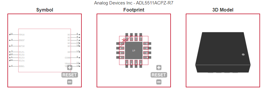
| ADL5511ACPZ-R7 ECAD MODELS |
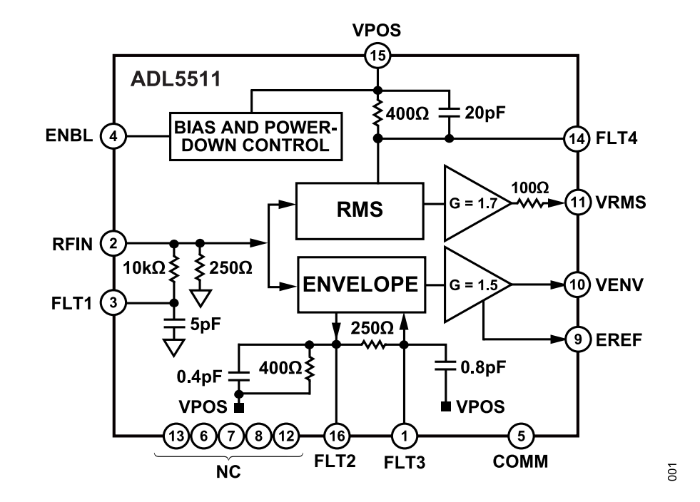
| ADL5511ACPZ-R7 FUNCTIONAL BLOCK DIAGRAM
|
| ADL5511ACPZ-R7 APPLICATIONS
|
| |
| COUNTRY OF ORIGIN |
| China |
| United States of America |
| |
| PARAMETRIC INFO |
| Frequency Band (MHz) |
0 to 6000 |
| Minimum Operating Supply Voltage (V) |
4.75 |
| Typical Supply Current (mA) |
21.5 |
| Maximum Operating Supply Voltage (V) |
5.25 |
| Maximum Power Dissipation (mW) |
580 |
| Typical Output Current (mA) |
15 |
| Maximum Output Voltage (V) |
3.8(Typ) |
| Minimum Operating Temperature (°C) |
-40 |
| Maximum Operating Temperature (°C) |
85 |
| Minimum Storage Temperature (°C) |
-65 |
| Maximum Storage Temperature (°C) |
150 |
| Thermal Resistance (°C/W) |
68.9 |
|
| |
| PACKAGE INFO |
| Supplier Package |
LFCSP EP |
| Basic Package Type |
Non-Lead-Frame SMT |
| Pin Count |
16 |
| Lead Shape |
No Lead |
| PCB |
16 |
| Tab |
N/R |
| Pin Pitch (mm) |
0.5 |
| Package Length (mm) |
3 |
| Package Width (mm) |
3 |
| Package Height (mm) |
0.73 |
| Package Diameter (mm) |
N/R |
| Package Overall Length (mm) |
3 |
| Package Overall Width (mm) |
3 |
| Package Overall Height (mm) |
0.75 |
| Seated Plane Height (mm) |
0.75 |
| Mounting |
Surface Mount |
| Package Weight (g) |
N/A |
| Package Material |
Plastic |
| Package Description |
Lead Frame Chip Scale Package, Exposed Pad |
| Package Family Name |
CSP |
| Jedec |
MO-220WEED-6 |
| Package Outline |
Link to Datasheet |
|
| |
| MANUFACTURING INFO |
| MSL |
3 |
| Maximum Reflow Temperature (°C) |
260 |
| Reflow Solder Time (Sec) |
30 |
| Number of Reflow Cycle |
3 |
| Standard |
J-STD-020D |
| Maximum Wave Temperature (°C) |
N/R |
| Wave Solder Time (Sec) |
N/R |
| Lead Finish(Plating) |
Matte Sn annealed |
| Under Plating Material |
Ag |
| Terminal Base Material |
Cu Alloy |
| Number of Wave Cycles |
N/R |
|
| |
| PACKAGING INFO |
| Packaging Suffix |
R7 |
| Packaging |
Tape and Reel |
| Quantity Of Packaging |
1500 |
| Reel Diameter (in) |
7 |
| Tape Pitch (mm) |
8 |
| Tape Width (mm) |
12 |
| Component Orientation |
Q2 |
| Packaging Document |
Link to Datasheet |
| Tape Material |
Plastic |
| Tape Type |
Embossed |
|
| |
| ECAD MODELS |
 |
| |
| FUNCTIONAL BLOCK DIAGRAM
|
 |
|
| APPLICATIONS
|
| ► RMS power and envelope detection of W-CDMA, CDMA2000,
LTE, and other complex waveforms |
| ► Drain modulation based power amplifier linearization |
| ► Power amplifier linearization employing envelope-tracking methods |
|