 |
||||||||||||||||||||||||||||||||||||||||||||||||||||||||
| • Input voltage range: 4.5 V to 16 V |
||||||||||||||||||||||||||||||||||||||||||||||||||||||||
| • Maximum output current: 800 mA |
||||||||||||||||||||||||||||||||||||||||||||||||||||||||
| • Low noise 1.0 µV rms total integrated noise from 100 Hz to 100 kHz 1.6 µV rms total integrated noise from 10 Hz to 100 kHz |
||||||||||||||||||||||||||||||||||||||||||||||||||||||||
| • Noise spectral density: 1.7 nV√Hz typical from 10 kHz to 1 MHz |
||||||||||||||||||||||||||||||||||||||||||||||||||||||||
| • Power supply rejection ratio (PSRR) at 400 mA load >90 dB from 1 kHz to 100 kHz, VOUT = 5 V >60 dB at 1 MHz, VOUT = 5 V |
||||||||||||||||||||||||||||||||||||||||||||||||||||||||
| • Dropout voltage: 0.6 V at VOUT = 5 V, 800 mA load |
||||||||||||||||||||||||||||||||||||||||||||||||||||||||
| • Initial voltage accuracy: ±1% |
||||||||||||||||||||||||||||||||||||||||||||||||||||||||
| • Voltage accuracy over line, load and temperature: ±2% |
||||||||||||||||||||||||||||||||||||||||||||||||||||||||
| • Quiescent current (IGND): 4.3 mA at no load |
||||||||||||||||||||||||||||||||||||||||||||||||||||||||
| • Low shutdown current: 0.1 µA |
||||||||||||||||||||||||||||||||||||||||||||||||||||||||
| • Stable with a 10 µF ceramic output capacitor |
||||||||||||||||||||||||||||||||||||||||||||||||||||||||
| • Fixed output voltage options: 1.8 V, 2.8 V, 3.0 V, 3.3 V, 4.5 V, 4.8 V, and 5.0 V (16 outputs between 1.5 V and 5.0 V areavailable) |
||||||||||||||||||||||||||||||||||||||||||||||||||||||||
| • Exposed pad 8-lead LFCSP and 8-lead SOIC packages |
||||||||||||||||||||||||||||||||||||||||||||||||||||||||
| CATALOG | ||||||||||||||||||||||||||||||||||||||||||||||||||||||||
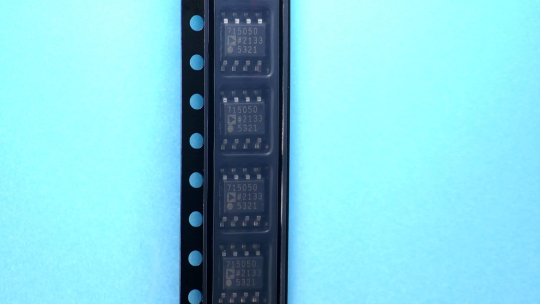
| ADM7150ARDZ-5.0-R7 COUNTRY OF ORIGIN |
||||||||||||||||||||||||||||||||||||||||||||||||||||||||
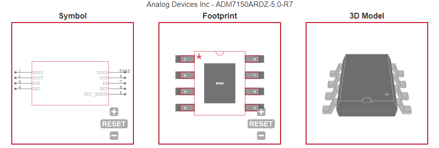
| ADM7150ARDZ-5.0-R7 PARAMETRIC INFO |
||||||||||||||||||||||||||||||||||||||||||||||||||||||||
| ADM7150ARDZ-5.0-R7 PACKAGE INFO |
||||||||||||||||||||||||||||||||||||||||||||||||||||||||
| ADM7150ARDZ-5.0-R7 MANUFACTURING INFO |
||||||||||||||||||||||||||||||||||||||||||||||||||||||||
| ADM7150ARDZ-5.0-R7 PACKAGING INFO |
||||||||||||||||||||||||||||||||||||||||||||||||||||||||
| ADM7150ARDZ-5.0-R7 ECAD MODELS |
||||||||||||||||||||||||||||||||||||||||||||||||||||||||
| ADM7150ARDZ-5.0-R7 APPLICATIONS |
||||||||||||||||||||||||||||||||||||||||||||||||||||||||
| COUNTRY OF ORIGIN |
||||||||||||||||||||||||||||||||||||||||||||||||||||||||
| Philippines |
||||||||||||||||||||||||||||||||||||||||||||||||||||||||
| PARAMETRIC INFO |
||||||||||||||||||||||||||||||||||||||||||||||||||||||||
|
||||||||||||||||||||||||||||||||||||||||||||||||||||||||
| PACKAGE INFO |
||||||||||||||||||||||||||||||||||||||||||||||||||||||||
|
||||||||||||||||||||||||||||||||||||||||||||||||||||||||
| MANUFACTURING INFO |
||||||||||||||||||||||||||||||||||||||||||||||||||||||||
|
||||||||||||||||||||||||||||||||||||||||||||||||||||||||
| PACKAGING INFO |
||||||||||||||||||||||||||||||||||||||||||||||||||||||||
|
||||||||||||||||||||||||||||||||||||||||||||||||||||||||
| ECAD MODELS |
||||||||||||||||||||||||||||||||||||||||||||||||||||||||
 |
||||||||||||||||||||||||||||||||||||||||||||||||||||||||
| APPLICATIONS |
||||||||||||||||||||||||||||||||||||||||||||||||||||||||
| • Regulated power noise sensitive applications RF mixers, phase-locked loops (PLLs), voltage-controlled oscillators (VCOs), and PLLs with integrated VCOs |
||||||||||||||||||||||||||||||||||||||||||||||||||||||||
| • Communications and infrastructure |
||||||||||||||||||||||||||||||||||||||||||||||||||||||||
| • Cable digital-to-analog converter (DAC) drivers |
||||||||||||||||||||||||||||||||||||||||||||||||||||||||
| • Backhaul and microwave links |
||||||||||||||||||||||||||||||||||||||||||||||||||||||||