|
|
• Input voltage range: 2.3 V to 5.5 V
|
• Maximum load current: 600 mA
|
• Noise spectral density: 1.5 nV/√Hz from 10 kHz to 1 MHz
|
• Dropout voltage: 120 mV typical at VOUT = 3.3 V, IOUT = 600 mA
|
• Initial accuracy: ±0.5%
|
|
| CATALOG |
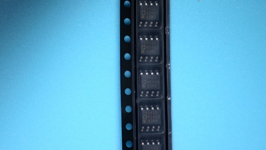
ADM7154ARDZ-3.3-R7 COUNTRY OF ORIGIN
|
ADM7154ARDZ-3.3-R7 PARAMETRIC INFO
|
ADM7154ARDZ-3.3-R7 PACKAGE INFO
|
ADM7154ARDZ-3.3-R7 MANUFACTURING INFO
|
ADM7154ARDZ-3.3-R7 PACKAGING INFO
|
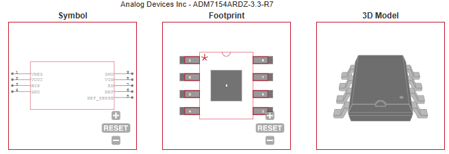
ADM7154ARDZ-3.3-R7 ECAD MODELS
|
ADM7154ARDZ-3.3-R7 APPLICATIONS
|
|
COUNTRY OF ORIGIN
|
Philippines
|
|
PARAMETRIC INFO
|
| Type |
LDO |
| Number of Outputs |
1 |
| Maximum Output Current (A) |
0.6 |
| Minimum Operating Temperature (°C) |
-40 |
| Maximum Operating Temperature (°C) |
125 |
| Output Type |
Fixed |
| Output Voltage Range (V) |
1.8 to 10 |
| Junction to Ambient |
36.9°C/W |
| Junction to Case |
27.1°C/W |
| Polarity |
Positive |
| Special Features |
Current Limit|Thermal Overload Protection |
| Load Regulation |
0.3%/A(Typ) |
| Line Regulation |
0.02%/V |
| Maximum Dropout Voltage @ Current (V) |
0.13@400mA|0.21@600mA |
| Minimum Input Voltage (V) |
2.3 |
| Maximum Input Voltage (V) |
5.5 |
| Output Voltage (V) |
3.3 |
| Typical Quiescent Current (mA) |
4 |
| Typical Dropout Voltage @ Current (V) |
0.08@400mA|0.12@600mA |
| Accuracy (%) |
±0.5 |
| Minimum Storage Temperature (°C) |
-65 |
| Maximum Storage Temperature (°C) |
150 |
| Noise Spectral Density (uV/rtHz) |
1.5@1000kHz |
| Typical PSRR (dB) |
90 |
| Typical Output Capacitance (uF) |
10 |
| Typical Output Noise Voltage (uVrms) |
1.6 |
| Pass Element Type |
PMOS |
| Output Capacitor Type |
Ceramic |
|
|
PACKAGE INFO
|
| Supplier Package |
SOIC N EP |
| Basic Package Type |
Lead-Frame SMT |
| Pin Count |
8 |
| Lead Shape |
Gull-wing |
| PCB |
8 |
| Tab |
N/R |
| Package Length (mm) |
4.9 |
| Package Width (mm) |
3.9 |
| Package Height (mm) |
1.65(Max) |
| Package Diameter (mm) |
N/R |
| Mounting |
Surface Mount |
| Package Material |
Plastic |
| Package Description |
Small Outline IC Narrow Body, Exposed Pad |
| Package Family Name |
SO |
| Jedec |
MS-012AA |
| Package Outline |
Link to Datasheet |
|
|
MANUFACTURING INFO
|
| MSL |
3 |
| Maximum Reflow Temperature (°C) |
260 |
| Reflow Solder Time (Sec) |
30 |
| Number of Reflow Cycle |
3 |
| Standard |
J-STD-020D |
| Maximum Wave Temperature (°C) |
N/R |
| Wave Solder Time (Sec) |
N/R |
| Lead Finish(Plating) |
Matte Sn annealed |
| Under Plating Material |
Ag |
| Terminal Base Material |
Cu Alloy |
|
|
PACKAGING INFO
|
| Packaging Suffix |
R7 |
| Packaging |
Tape and Reel |
| Quantity Of Packaging |
1000 |
| Reel Diameter (in) |
7 |
| Packaging Document |
Link to Datasheet |
|
|
ECAD MODELS
|
|
|
| APPLICATIONS |
| • Regulation to noise sensitive applications: PLLs, VCOs, and PLLs with integrated VCOs |
| • Communications and infrastructure |
| • Backhaul and microwave links |
| |