|
|
| CATALOG |
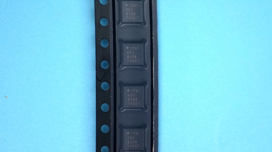
ADP1741ACPZ-R7 COUNTRY OF ORIGIN
|
ADP1741ACPZ-R7 PARAMETRIC INFO
|
ADP1741ACPZ-R7 PACKAGE INFO
|
ADP1741ACPZ-R7 MANUFACTURING INFO
|
ADP1741ACPZ-R7 PACKAGING INFO
|
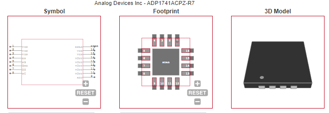
ADP1741ACPZ-R7 ECAD MODELS
|
ADP1741ACPZ-R7 APPLICATIONS
|
|
COUNTRY OF ORIGIN
|
Korea (Republic of)
|
Taiwan (Province of China)
|
|
PARAMETRIC INFO
|
| Type |
LDO |
| Number of Outputs |
1 |
| Maximum Output Current (A) |
2 |
| Minimum Operating Temperature (°C) |
-40 |
| Maximum Operating Temperature (°C) |
125 |
| Output Type |
Adjustable |
| Output Voltage Range (V) |
<1.8|1.8 to 10 |
| Regulation Condition Change In Load |
1.99A |
| Junction to Ambient |
130°C/W |
| Polarity |
Positive |
| Special Features |
Current Limit|Thermal Protection |
| Process Technology |
CMOS |
| Load Regulation |
0.5%/A |
| Line Regulation |
0.3%/V |
| Maximum Dropout Voltage @ Current (V) |
0.018@100mA|0.28@2A |
| Minimum Input Voltage (V) |
1.6 |
| Maximum Input Voltage (V) |
3.6 |
| Output Voltage (V) |
0.75 to 3.3 |
| Typical Dropout Voltage @ Current (V) |
0.01@100mA|0.16@2A |
| Accuracy (%) |
±1 |
| Minimum Storage Temperature (°C) |
-65 |
| Maximum Storage Temperature (°C) |
150 |
| Typical Ground Current @ Full Load (mA) |
1.5 |
| Typical PSRR (dB) |
65 |
| Typical Output Capacitance (uF) |
4.7 |
| Typical Output Noise Voltage (uVrms) |
23 |
| Pass Element Type |
PMOS |
| Output Capacitor Type |
Ceramic |
|
|
PACKAGE INFO
|
| Supplier Package |
LFCSP EP |
| Basic Package Type |
Non-Lead-Frame SMT |
| Pin Count |
16 |
| Lead Shape |
No Lead |
| PCB |
16 |
| Tab |
N/R |
| Pin Pitch (mm) |
0.65 |
| Package Length (mm) |
4 |
| Package Width (mm) |
4 |
| Package Height (mm) |
0.73 |
| Package Diameter (mm) |
N/R |
| Package Overall Length (mm) |
4 |
| Package Overall Width (mm) |
4 |
| Package Overall Height (mm) |
0.75 |
| Seated Plane Height (mm) |
0.75 |
| Mounting |
Surface Mount |
| Package Weight (g) |
N/A |
| Package Material |
Plastic |
| Package Description |
Lead Frame Chip Scale Package, Exposed Pad |
| Package Family Name |
CSP |
| Jedec |
MO-220WGGC |
| Package Outline |
Link to Datasheet |
|
|
| MANUFACTURING INFO |
| MSL |
3 |
| Maximum Reflow Temperature (°C) |
260 |
| Reflow Solder Time (Sec) |
30 |
| Number of Reflow Cycle |
3 |
| Standard |
J-STD-020D |
| Maximum Wave Temperature (°C) |
N/R |
| Wave Solder Time (Sec) |
N/R |
| Wave Temp. Source |
Link to Datasheet |
| Lead Finish(Plating) |
Matte Sn annealed |
| Under Plating Material |
Ag |
| Terminal Base Material |
Cu Alloy |
| Number of Wave Cycles |
N/R |
|
| |
PACKAGING INFO
|
| Packaging Suffix |
R7 |
| Packaging |
Tape and Reel |
| Quantity Of Packaging |
1500 |
| Reel Diameter (in) |
7 |
| Tape Pitch (mm) |
8 |
| Tape Width (mm) |
12 |
| Component Orientation |
Q2 |
| Packaging Document |
Link to Datasheet |
| Tape Material |
Plastic |
| Tape Type |
Embossed |
|
|
ECAD MODELS
|
|
|
APPLICATIONS
|
• Server computers
|
• Memory components
|
• Telecommunications equipment
|
• Network equipment
|
• DSP/FPGA/microprocessor supplies
|
• Instrumentation equipment/data acquisition systems
|
|