|
|
• 3 A maximum output current
|
• Fixed output voltage range: VOUT_FIXED = 0.9 V to 1.5 V
|
• Adjustable output voltage range: VOUT_ADJ = 0.5 V to 1.5 V
|
• Ultralow noise: 2 µV rms, 100 Hz to 100 kHz
|
• Low dropout voltage: 95 mV typical at 3 A load
|
|
| CATALOG |
ADP1763ACPZ-0.9-R7 COUNTRY OF ORIGIN
|
ADP1763ACPZ-0.9-R7 PARAMETRIC INFO
|
ADP1763ACPZ-0.9-R7 PACKAGE INFO
|
ADP1763ACPZ-0.9-R7 MANUFACTURING INFO
|
ADP1763ACPZ-0.9-R7 PACKAGING INFO
|
ADP1763ACPZ-0.9-R7 ECAD MODELS
|
ADP1763ACPZ-0.9-R7 APPLICATIONS
|
|
COUNTRY OF ORIGIN
|
Korea (Republic of)
|
|
PARAMETRIC INFO
|
| Type |
LDO |
| Number of Outputs |
1 |
| Maximum Output Current (A) |
3 |
| Minimum Operating Temperature (°C) |
-40 |
| Maximum Operating Temperature (°C) |
125 |
| Output Type |
Fixed |
| Output Voltage Range (V) |
<1.8 |
| Regulation Condition Change In Load |
2.99A |
| Regulation Condition Change In Line |
0.88V |
| Junction to Ambient |
56°C/W |
| Polarity |
Positive |
| Special Features |
Current Limit|Thermal Protection |
| Load Regulation |
0.12%/A(Typ) |
| Process Technology |
CMOS |
| Line Regulation |
0.15%/V |
| Maximum Dropout Voltage @ Current (V) |
0.023@100mA|0.145@3A |
| Minimum Input Voltage (V) |
1.1 |
| Maximum Input Voltage (V) |
1.98 |
| Output Voltage (V) |
0.9 |
| Typical Dropout Voltage @ Current (V) |
0.095@3A |
| Accuracy (%) |
±1.5 |
| Minimum Storage Temperature (°C) |
-65 |
| Maximum Storage Temperature (°C) |
150 |
| Typical Ground Current @ Full Load (mA) |
12 |
| Noise Spectral Density (uV/rtHz) |
0.004@10kHz |
| Typical PSRR (dB) |
62 |
| Typical Output Capacitance (uF) |
10(Min) |
| Typical Output Noise Voltage (uVrms) |
12 |
| Output Capacitor Type |
Ceramic |
|
|
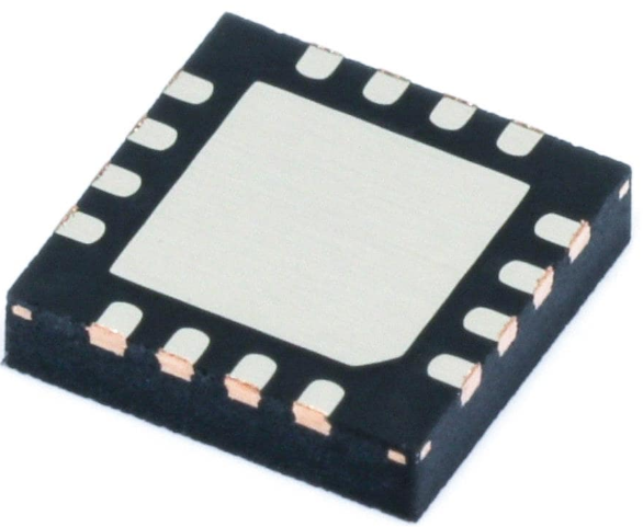
PACKAGE INFO
|
| Supplier Package |
LFCSP EP |
| Basic Package Type |
Non-Lead-Frame SMT |
| Pin Count |
16 |
| Lead Shape |
No Lead |
| PCB |
16 |
| Tab |
N/R |
| Pin Pitch (mm) |
0.5 |
| Package Length (mm) |
3 |
| Package Width (mm) |
3 |
| Package Height (mm) |
0.73 |
| Package Diameter (mm) |
N/R |
| Package Overall Length (mm) |
3 |
| Package Overall Width (mm) |
3 |
| Package Overall Height (mm) |
0.75 |
| Seated Plane Height (mm) |
0.75 |
| Mounting |
Surface Mount |
| Package Weight (g) |
N/A |
| Package Material |
Plastic |
| Package Description |
Lead Frame Chip Scale Package, Exposed Pad |
| Package Family Name |
CSP |
| Jedec |
MO-220WEED-6 |
| Package Outline |
Link to Datasheet |
|
|
MANUFACTURING INFO
|
| MSL |
3 |
| Maximum Reflow Temperature (°C) |
260 |
| Reflow Solder Time (Sec) |
30 |
| Number of Reflow Cycle |
3 |
| Standard |
J-STD-020D |
| Lead Finish(Plating) |
Matte Sn annealed |
| Under Plating Material |
Ag |
| Terminal Base Material |
Cu Alloy |
|
|
PACKAGING INFO
|
| Packaging Suffix |
R7 |
| Packaging |
Tape and Reel |
| Quantity Of Packaging |
1500 |
|
|
ECAD MODELS
|
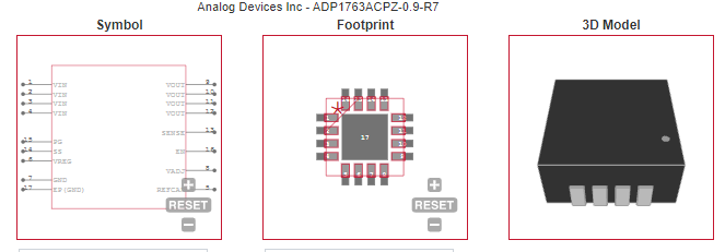
|
|
| APPLICATIONS |
| • Regulation to noise sensitive applications such as RF transceivers, analog-to-digital converter (ADC) and digital-to-analog converter(DAC)circuits, phase-locked loops (PLLs), voltage controlled oscillators (VCOs) and clocking integrated circuits |
| • Field-programmable gate array (FPGA) and digital signal processor (DSP) supplies |
| • Medical and healthcare |
| • Industrial and instrumentation |
| • Automotive |
| |