|
|
| • isoPower integrated, isolated dc-to-dc converter |
| • Qualified for automotive applications |
| • Regulated 5 V or 3.3 V output |
| • Up to 500 mW output power |
| • Quad dc-to-25 Mbps (NRZ) signal isolation channels |
| • 16-lead SOIC package with 7.6 mm creepage |
| • High temperature operation: 105°C |
| • High common-mode transient immunity: >25 kV/µs |
| • Safety and regulatory approvals
UL recognition: 2500 V rms for 1 minute per UL 1577
CSA Component Acceptance Notice #5A
VDE certificate of conformity
DIN EN 69747-5-2 (VDE 0884 Teil 2):2003-1
VIORM = 565 V peak |
|
| CATALOG |
| ADuM5401WCRWZ-1-RL COUNTRY OF ORIGIN |
| ADuM5401WCRWZ-1-RL PARAMETRIC INFO |
| ADuM5401WCRWZ-1-RL PACKAGE INFO |
| ADuM5401WCRWZ-1-RL MANUFACTURING INFO |
| ADuM5401WCRWZ-1-RL PACKAGING INFO |
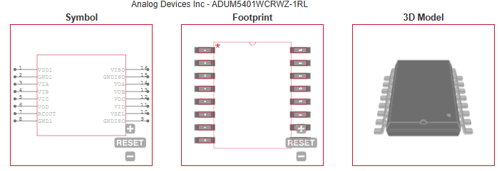
ADuM5401WCRWZ-1-RL ECAD MODELS
|
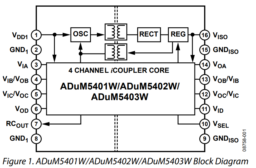
| ADuM5401WCRWZ-1-RL FUNCTIONAL BLOCK DIAGRAM |
| ADuM5401WCRWZ-1-RL APPLICATIONS |
|
| COUNTRY OF ORIGIN |
| Malaysia |
Ireland
|
Taiwan (Province of China)
|
|
| PARAMETRIC INFO |
| Number of Channels per Chip |
4 |
| Type |
General Purpose |
| Isolated Power |
Yes |
| Output Type |
CMOS |
| Minimum Isolation Voltage (Vrms) |
2500 |
| Maximum Power Dissipation (mW) |
500 |
| Minimum Pulse Width (ns) |
40 |
| Maximum Pulse Width Distortion (ns) |
6 |
| Minimum Common Mode Rejection (kV/us) |
25 |
| Maximum Working Insulation Voltage |
565Vp |
| Maximum Fall Time (ns) |
2.5(Typ) |
| Maximum Rise Time (ns) |
2.5(Typ) |
| Maximum Propagation Delay Time (tPHL) (ns) |
60 |
| Maximum Propagation Delay Time (tPLH) (ns) |
60 |
| Maximum Propagation Delay Skew (ns) |
45 |
| Maximum Data Rate |
25Mbps |
| Minimum Operating Supply Voltage (V) |
3 |
| Maximum Operating Supply Voltage (V) |
5.5 |
| Minimum Operating Temperature (°C) |
-40 |
| Maximum Operating Temperature (°C) |
105 |
| Supplier Temperature Grade |
Industrial |
| Coupling Type |
Magnetic Coupling |
| Forward/Reverse Channels |
3/1 |
| Minimum Storage Temperature (°C) |
-55 |
| Maximum Storage Temperature (°C) |
150 |
|
|
| PACKAGE INFO |
| Supplier Package |
SOIC W |
| Basic Package Type |
Lead-Frame SMT |
| Pin Count |
16 |
| Lead Shape |
Gull-wing |
| PCB |
16 |
| Tab |
N/R |
| Pin Pitch (mm) |
1.27 |
| Package Length (mm) |
10.5(Max) |
| Package Width (mm) |
7.6(Max) |
| Package Height (mm) |
2.35(Max) |
| Package Diameter (mm) |
N/R |
| Package Overall Length (mm) |
10.5(Max) |
| Package Overall Width (mm) |
10.65(Max) |
| Package Overall Height (mm) |
2.65(Max) |
| Seated Plane Height (mm) |
2.65(Max) |
| Mounting |
Surface Mount |
| Package Weight (g) |
N/A |
| Package Material |
Plastic |
| Package Description |
Small Outline IC Wide Body |
| Package Family Name |
SO |
| Jedec |
MS-013AA |
| Package Outline |
Link to Datasheet |
|
|
| MANUFACTURING INFO |
| MSL |
3 |
| Maximum Reflow Temperature (°C) |
260 |
| Reflow Solder Time (Sec) |
30 |
| Number of Reflow Cycle |
3 |
| Standard |
J-STD-020D |
| Maximum Wave Temperature (°C) |
N/R |
| Wave Solder Time (Sec) |
N/R |
| Lead Finish(Plating) |
Matte Sn annealed |
| Under Plating Material |
Ag |
| Terminal Base Material |
Cu Alloy |
|
|
| PACKAGING INFO |
| Packaging Suffix |
RL |
| Packaging |
Tape and Reel |
| Reel Diameter (in) |
13 |
| Packaging Document |
Link to Datasheet |
|
|
| ECAD MODELS |
|
|
| FUNCTIONAL BLOCK DIAGRAM |
|
|
| APPLICATIONS |
| • Hybrid electric battery management |
|