|
|
• AEC-Q100 qualified for automotive applications:– Temperature grade 1: –40°C to +125°C, TA
|
• Functional-Safety Capable– Documentation available to aid functional safety system design
|
• Low offset voltage: 1 mV (typical)
|
• High output current drive: 400 mA, continuous (per channel)– Replaces discrete op amps and transistors
|
• Wide supply range for both supplies (up to 16 V)
|
• Overtemperature shutdown
|
• Current limit
|
• Shutdown pin for low IQ applications
|
• Stable with large capacitive loads
|
• 2-MHz gain bandwidth with 3.4-V/µs slew rate
|
• Internal RF/EMI filter
|
• Package: 14-pin HTSSOP (PWP)
|
|
| CATALOG |
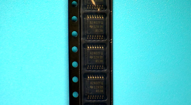
ALM2402FQPWPRQ1 COUNTRY OF ORIGIN
|
ALM2402FQPWPRQ1 PARAMETRIC INFO
|
ALM2402FQPWPRQ1 PACKAGE INFO
|
ALM2402FQPWPRQ1 MANUFACTURING INFO
|
ALM2402FQPWPRQ1 PACKAGING INFO
|
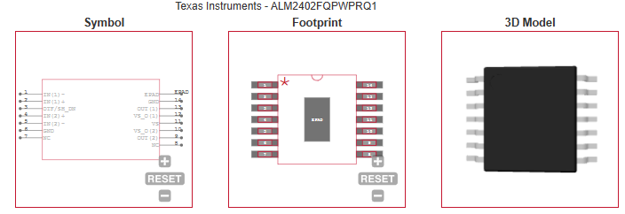
ALM2402FQPWPRQ1 ECAD MODELS
|
ALM2402FQPWPRQ1 APPLICATIONS
|
|
COUNTRY OF ORIGIN
|
Malaysia
|
|
PARAMETRIC INFO
|
| Manufacturer Type |
Power Amplifier |
| Type |
Power Amplifier |
| Rail to Rail |
Rail to Rail Output |
| Minimum Single Supply Voltage (V) |
4.5 |
| Number of Channels per Chip |
2 |
| Minimum PSRR (dB) |
82 |
| Typical Single Supply Voltage (V) |
5|9|12|15 |
| Maximum Single Supply Voltage (V) |
16 |
| Maximum Quiescent Current (mA) |
9@5V |
| Typical Gain Bandwidth Product (MHz) |
1.3 |
| Maximum Input Offset Voltage (mV) |
7@5V |
| Maximum Input Offset Current (uA) |
0.002@5V |
| Maximum Operating Supply Voltage (V) |
16 |
| Maximum Input Bias Current (uA) |
0.002@5V |
| Minimum CMRR (dB) |
80 |
| Maximum Supply Voltage Range (V) |
16 to 17 |
| Minimum CMRR Range (dB) |
80 to 85 |
| Typical Voltage Gain (dB) |
93 |
| Typical Slew Rate (V/us) |
1.7@5V |
| Typical Settling Time (ns) |
2000 |
| Typical Output Current (mA) |
400(Max) |
| Typical Input Noise Voltage Density (nV/rtHz) |
115@5V |
| Typical Input Bias Current (uA) |
0.0005@5V |
| Shut Down Support |
Yes |
| Minimum Operating Temperature (°C) |
-40 |
| Maximum Operating Temperature (°C) |
125 |
| Supplier Temperature Grade |
Automotive |
| Power Supply Type |
Single|Dual |
|
|
PACKAGE INFO
|
| Supplier Package |
HTSSOP EP |
| Basic Package Type |
Lead-Frame SMT |
| Pin Count |
14 |
| Lead Shape |
Gull-wing |
| PCB |
14 |
| Tab |
N/R |
| Pin Pitch (mm) |
0.65 |
| Package Length (mm) |
5.1(Max) |
| Package Width (mm) |
4.5(Max) |
| Package Height (mm) |
1.05(Max) |
| Package Diameter (mm) |
N/R |
| Package Overall Length (mm) |
5.1(Max) |
| Package Overall Width (mm) |
6.6(Max) |
| Package Overall Height (mm) |
1.2(Max) |
| Seated Plane Height (mm) |
1.2(Max) |
| Mounting |
Surface Mount |
| Package Weight (g) |
N/A |
| Package Material |
Plastic |
| Package Description |
Heat Sinked Thin Shrink Small Outline Package, Exposed Pad |
| Package Family Name |
SO |
| Jedec |
MO-153ABT-1 |
| Package Outline |
Link to Datasheet |
|
|
MANUFACTURING INFO
|
| MSL |
3 |
| Maximum Reflow Temperature (°C) |
260 |
| Reflow Solder Time (Sec) |
30 |
| Number of Reflow Cycle |
3 |
| Standard |
J-STD-020D |
| Reflow Temp. Source |
Link to Datasheet |
| Maximum Wave Temperature (°C) |
N/R |
| Wave Solder Time (Sec) |
N/R |
| Wave Temp. Source |
Link to Datasheet |
| Lead Finish(Plating) |
Au |
| Under Plating Material |
Pd over Ni |
| Terminal Base Material |
Cu Alloy |
| Number of Wave Cycles |
N/R |
|
|
PACKAGING INFO
|
| Packaging |
Tape and Reel |
| Quantity Of Packaging |
2000 |
| Packaging Document |
Link to Datasheet |
|
|
| ECAD MODELS |
|
|
| APPLICATIONS |
• Resolver-based automotive applications
|
• Inverter and motor control
|
| • Brake system |
| • Electric power steering (EPS) |
| • Rearview mirror module |
| • Automotive eMirrors |
| • Servo drive power stage module |
| |