 |
|
• Low-voltage Operation
̶ VCC = 1.7V to 5.5V |
| • Internally Organized as 128 x 8 (1K) or 256 x 8 (2K) |
| • I
2
C Compatible (2-wire) Serial Interface |
| • Schmitt Trigger, Filtered Inputs for Noise Suppression |
| • Bidirectional Data Transfer Protocol |
| • 400kHz (1.7V) and 1MHz (2.5V, 2.7V, 5.0V) Compatibility |
| • Write Protect Pin for Hardware Data Protection |
• 8-byte Page Write Mode
̶ Partial Page Writes Allowed |
| • Self-timed Write Cycle (5ms max) |
• High-reliability
̶ Endurance: 1,000,000 Write Cycles
̶ Data Retention: 100 Years |
• Green Package Options (Pb/Halide-free/RoHS-compliant)
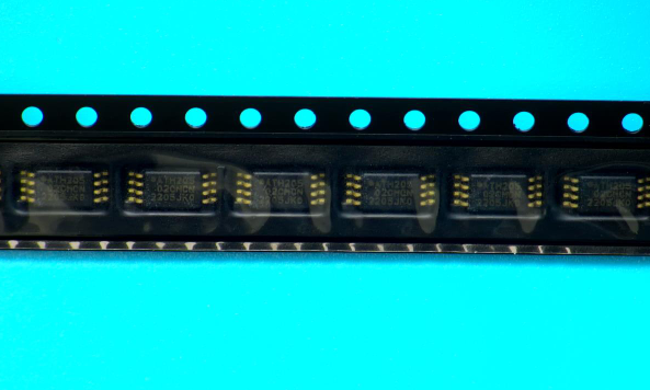
̶ 8-lead PDIP, 8-lead JEDEC SOIC, 8-lead TSSOP, 8-pad UDFN, 5-lead
SOT23, and 8-ball VFBGA |
| • Die Sale Options: Wafer Form and Tape and Reel Available |
|
| CATALOG |
| AT24C02C-XHM-T COUNTRY OF ORIGIN
|
| AT24C02C-XHM-T PARAMETRIC INFO |
| AT24C02C-XHM-T PACKAGE INFO |
| AT24C02C-XHM-T MANUFACTURING INFO |
| AT24C02C-XHM-T PACKAGING INFO |
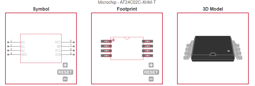
| AT24C02C-XHM-T ECAD MODELS |
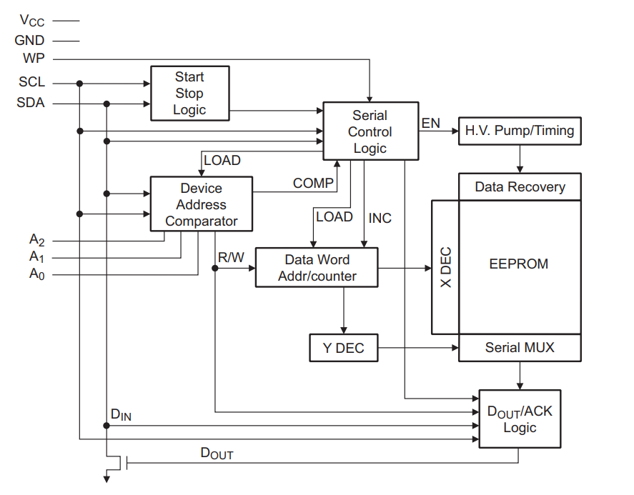
| AT24C02C-XHM-T FUNCTIONAL BLOCK DIAGRAM |
|
| COUNTRY OF ORIGIN |
| Philippines |
| Singapore |
| Thailand |
| Malaysia |
| China |
| Taiwan (Province of China) |
|
| PARAMETRIC INFO |
| Density (bit) |
2K |
| Interface Type |
Serial-I2C |
| Maximum Operating Frequency (MHz) |
1 |
| Maximum Access Time (ns) |
550 |
| Typical Operating Supply Voltage (V) |
1.8|2.5|3.3|5 |
| Minimum Operating Temperature (°C) |
-40 |
| Maximum Operating Temperature (°C) |
85 |
| Supplier Temperature Grade |
Industrial |
| Programmability |
Yes |
| Density in Bits (bit) |
2048 |
| Maximum Operating Current (mA) |
3 |
| Hardware Data Protection |
Yes |
| Organization |
256x8 |
| Data Retention (Year) |
100 |
| Minimum Operating Supply Voltage (V) |
1.7 |
| Maximum Operating Supply Voltage (V) |
5.5 |
| Minimum Storage Temperature (°C) |
-65 |
| Number of Bits per Word (bit) |
8 |
| Maximum Storage Temperature (°C) |
150 |
| Address Bus Width (bit) |
3 |
|
|
| PACKAGE INFO |
| Supplier Package |
TSSOP |
| Basic Package Type |
Lead-Frame SMT |
| Pin Count |
8 |
| Lead Shape |
Gull-wing |
| PCB |
8 |
| Tab |
N/R |
| Pin Pitch (mm) |
0.65 |
| Package Length (mm) |
3 |
| Package Width (mm) |
4.4 |
| Package Height (mm) |
1 |
| Package Diameter (mm) |
N/R |
| Package Overall Length (mm) |
3 |
| Package Overall Width (mm) |
6.4 |
| Package Overall Height (mm) |
1.2(Max) |
| Seated Plane Height (mm) |
1.2(Max) |
| Mounting |
Surface Mount |
| Package Weight (g) |
N/A |
| Package Material |
Plastic |
| Package Description |
Thin Shrink Small Outline Package |
| Package Family Name |
SO |
| Jedec |
MO-153AA |
| Package Outline |
Link to Datasheet |
|
|
| MANUFACTURING INFO |
| MSL |
1 |
| Maximum Reflow Temperature (°C) |
260 |
| Reflow Solder Time (Sec) |
20 to 40 |
| Number of Reflow Cycle |
3 |
| Standard |
J-STD-020C |
| Reflow Temp. Source |
Link to Datasheet |
| Maximum Wave Temperature (°C) |
N/R |
| Wave Solder Time (Sec) |
N/R |
| Lead Finish(Plating) |
Au |
| Under Plating Material |
Pd over Ni |
| Terminal Base Material |
Cu Alloy |
| Number of Wave Cycles |
N/R |
|
|
| PACKAGING INFO |
| Packaging Suffix |
T |
| Packaging |
Tape and Reel |
| Quantity Of Packaging |
5000 |
| Reel Diameter (in) |
13 |
| Reel Width (mm) |
12.4 |
| Tape Pitch (mm) |
8 |
| Tape Width (mm) |
12 |
| Feed Hole Pitch (mm) |
4 |
| Hole Center to Component Center (mm) |
2 |
| Component Orientation |
Q1 |
| Packaging Document |
Link to Datasheet |
| Tape Type |
Embossed |
|
|
| ECAD MODELS |
 |
|
| FUNCTIONAL BLOCK DIAGRAM |
 |
| |
| |