 |
|
• Write Protect Pin for Hardware Data Protection
– Utilizes Different Array Protection Compared to the AT24C02/04/08/16 |
• Low-voltage and Standard-voltage Operation
– 2.7 (VCC = 2.7V to 5.5V)
– 1.8 (VCC = 1.8V to 5.5V) |
| • Internally Organized 256 x 8 (2K), 512 x 8 (4K), 1024 x 8 (8K) or 2048 x 8 (16K) |
| • 2-wire Serial Interface
|
| • Schmitt Trigger, Filtered Inputs for Noise Suppression |
| • Bi-directional Data Transfer Protocol
|
| • 100 kHz (1.8V) and 400 kHz (2.5V, 2.7V, 5V) Clock Rate |
| • 8-byte Page (2K), 16-byte Page (4K, 8K, 16K) Write Modes |
| • Partial Page Writes are Allowed |
| • Self-timed Write Cycle (5 ms Max) |
• High Reliability
– Endurance: One Million Write Cycles
– Data Retention: 100 Years |
| • Automotive Grade, Extended Temperature and Lead-Free/Halogen-Free
Devices Available |
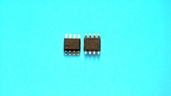
| • 8-lead PDIP, 8-lead JEDEC SOIC, 8-lead MAP and 8-lead TSSOP Packages |
|
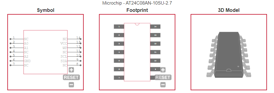
| CATALOG |
| AT24C08AN-10SU-2.7 COUNTRY OF ORIGIN |
| AT24C08AN-10SU-2.7 LIFECYCLE |
| AT24C08AN-10SU-2.7 PARAMETRIC INFO |
| AT24C08AN-10SU-2.7 PACKAGE INFO |
| AT24C08AN-10SU-2.7 MANUFACTURING INFO |
| AT24C08AN-10SU-2.7 ECAD MODELS |
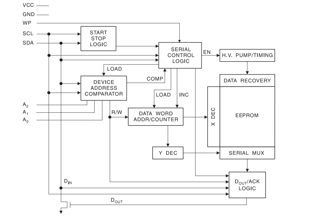
| AT24C08AN-10SU-2.7 FUNCTIONAL BLOCK DIAGRAM |
|
| COUNTRY OF ORIGIN |
| Philippines |
|
| LIFECYCLE |
Obsolete
May 19,2008 |
|
| PARAMETRIC INFO |
| Density (bit) |
8K |
| Interface Type |
Serial-2Wire |
| Maximum Operating Frequency (MHz) |
0.4 |
| Maximum Access Time (ns) |
900 |
| Typical Operating Supply Voltage (V) |
3.3|5 |
| Minimum Operating Temperature (°C) |
-40 |
| Maximum Operating Temperature (°C) |
85 |
| Supplier Temperature Grade |
Industrial |
| Programmability |
Yes |
| Density in Bits (bit) |
8192 |
| Maximum Operating Current (mA) |
3 |
| Hardware Data Protection |
Yes |
| Organization |
1Kx8 |
| Data Retention (Year) |
100 |
| Minimum Operating Supply Voltage (V) |
2.7 |
| Maximum Operating Supply Voltage (V) |
5.5 |
| Minimum Storage Temperature (°C) |
-65 |
| Maximum Storage Temperature (°C) |
150 |
| Number of Bits per Word (bit) |
8 |
| Address Bus Width (bit) |
3 |
|
| |
| PACKAGE INFO |
| Supplier Package |
SOIC N |
| Basic Package Type |
Lead-Frame SMT |
| Pin Count |
8 |
| Lead Shape |
Gull-wing |
| PCB |
8 |
| Tab |
N/R |
| Pin Pitch (mm) |
1.27 |
| Package Length (mm) |
4.98(Max) |
| Package Width (mm) |
3.99(Max) |
| Package Height (mm) |
1.48(Max) |
| Package Diameter (mm) |
N/R |
| Package Overall Length (mm) |
4.98(Max) |
| Package Overall Width (mm) |
6.2(Max) |
| Package Overall Height (mm) |
1.73(Max) |
| Seated Plane Height (mm) |
1.73(Max) |
| Mounting |
Surface Mount |
| Package Weight (g) |
N/A |
| Package Material |
Plastic |
| Package Description |
Small Outline IC Narrow Body |
| Package Family Name |
SO |
| Jedec |
MS-012AA |
| Package Outline |
Link to Datasheet |
|
| |
| MANUFACTURING INFO |
| MSL |
1|3 |
| Maximum Reflow Temperature (°C) |
260 |
| Reflow Solder Time (Sec) |
20 to 40 |
| Number of Reflow Cycle |
3 |
| Standard |
J-STD-020C |
| Reflow Temp. Source |
Link to Datasheet |
| Maximum Wave Temperature (°C) |
N/R |
| Wave Solder Time (Sec) |
N/R |
| Lead Finish(Plating) |
Matte Sn annealed |
| Under Plating Material |
N/A |
| Terminal Base Material |
Cu Alloy |
| Number of Wave Cycles |
N/R |
|
| |
| ECAD MODELS |
 |
|
| FUNCTIONAL BLOCK DIAGRAM |
 |
|