 |
|
| • Compatible with MCS®51 Products |
• 12K Bytes of In-System Programmable (ISP) Flash Program Memory
– SPI Serial Interface for Program Downloading
– Endurance: 10,000 Write/Erase Cycles
|
• 2K Bytes EEPROM Data Memory
– Endurance: 100,000 Write/Erase Cycles
|
| • 64-byte User Signature Array |
| • 2.7V to 5.5V Operating Range |
| • Fully Static Operation: 0 Hz to 24 MHz (in x1 and x2 Modes) |
| • Three-level Program Memory Lock |
| • 256 x 8-bit Internal RAM |
| • 32 Programmable I/O Lines
|
| • Three 16-bit Timer/Counters |
| • Nine Interrupt Sources |
| • Enhanced UART Serial Port with Framing Error Detection and Automatic
Address Recognition |
| • Enhanced SPI (Double Write/Read Buffered) Serial Interface |
| • Low-power Idle and Power-down Modes |
| • Interrupt Recovery from Power-down Mode |
| • Programmable Watchdog Timer |
| • Dual Data Pointer |
| • Power-off Flag |
• Flexible ISP Programming (Byte and Page Modes)
– Page Mode: 64 Bytes/Page for Code Memory, 32 Bytes/Page for Data Memory |
| • Four-level Enhanced Interrupt Controller |
| • Programmable and Fuseable x2 Clock Option |
| • Internal Power-on Reset |
| • 42-pin PDIP Package Option for Reduced EMC Emission |
| • Green (Pb/Halide-free) Packaging Option |
|
| CATALOG |
| AT89S8253-24AU COUNTRY OF ORIGIN |
| AT89S8253-24AU PARAMETRIC INFO |
| AT89S8253-24AU PACKAGE INFO |
| AT89S8253-24AU MANUFACTURING INFO |
| AT89S8253-24AU PACKAGING INFO |
| AT89S8253-24AU ECAD MODELS |
|
| COUNTRY OF ORIGIN |
| China |
| Philippines |
| Singapore |
| Taiwan (Province of China) |
| Thailand |
|
| PARAMETRIC INFO |
| Data Bus Width (bit) |
8 |
| Family Name |
AT89 |
| Device Core |
8051 |
| Instruction Set Architecture |
CISC |
| Maximum Clock Rate (MHz) |
24 |
| Program Memory Type |
Flash |
| Program Memory Size |
12KB |
| RAM Size |
256B |
| Maximum Expanded Memory Size |
64KB |
| EEPROM |
2KB |
| Direct Memory Access |
No |
| Floating Point Unit |
No |
| Bluetooth |
No |
| Wi-Fi |
No |
| Multiply Accumulate |
No |
| Internal/External Clock Type |
Internal/External |
| Touch Sensing Interface |
No |
| Power On Reset |
No |
| Memory Protection Unit |
No |
| Temperature Sensor |
No |
| DDR |
No |
| Memory Management Unit |
No |
| Integrated Development Environment |
No |
| Super Scalar |
No |
| External Bus Interface |
No |
| Maximum CPU Frequency (MHz) |
24 |
| Number of Programmable I/Os |
32 |
| Number of Timers |
3 |
| Core Architecture |
8051 |
| Watchdog |
1 |
| Parallel Master Port |
No |
| Real Time Clock |
No |
| Timers Resolution (bit) |
16/16/16 |
| Interface Type |
SPI/UART |
| Programmability |
Yes |
| SPI |
1 |
| I2C |
0 |
| Process Technology |
CMOS |
| I2S |
0 |
| UART |
1 |
| USART |
0 |
| CAN |
0 |
| USB |
0 |
| Ethernet |
0 |
| Minimum Operating Supply Voltage (V) |
2.7 |
| Typical Operating Supply Voltage (V) |
3.3|5 |
| Maximum Operating Supply Voltage (V) |
5.5 |
| Minimum Operating Temperature (°C) |
-40 |
| Maximum Operating Temperature (°C) |
85 |
| Temperature Flag |
Opr |
| Supplier Temperature Grade |
Industrial |
| Operating Supply Voltage (V) |
3.3|5 |
| Maximum Storage Temperature (°C) |
150 |
| Minimum Storage Temperature (°C) |
-65 |
|
| |
| PACKAGE INFO |
| Supplier Package |
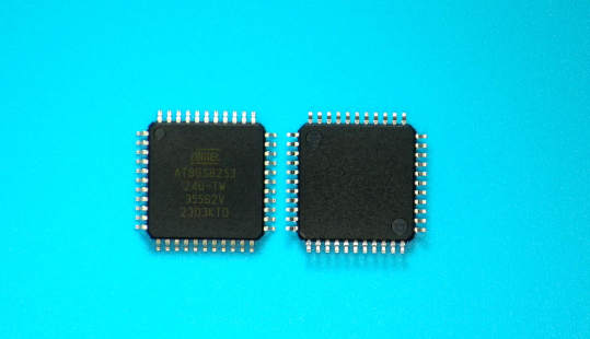
TQFP |
| Basic Package Type |
Lead-Frame SMT |
| Pin Count |
44 |
| Lead Shape |
Gull-wing |
| PCB |
44 |
| Tab |
N/R |
| Pin Pitch (mm) |
0.8 |
| Package Length (mm) |
10.1(Max) |
| Package Width (mm) |
10.1(Max) |
| Package Height (mm) |
1.05(Max) |
| Package Diameter (mm) |
N/R |
| Package Overall Length (mm) |
12.25(Max) |
| Package Overall Width (mm) |
12.25(Max) |
| Package Overall Height (mm) |
1.2(Max) |
| Seated Plane Height (mm) |
1.2(Max) |
| Mounting |
Surface Mount |
| Package Weight (g) |
N/A |
| Package Material |
Plastic |
| Package Description |
Thin Quad Flat Package |
| Package Family Name |
QFP |
| Jedec |
MS-026ACB |
| Package Outline |
Link to Datasheet |
|
| |
| MANUFACTURING INFO |
| MSL |
1|3 |
| Maximum Reflow Temperature (°C) |
260 |
| Reflow Solder Time (Sec) |
20 to 40 |
| Number of Reflow Cycle |
3 |
| Standard |
J-STD-020C |
| Reflow Temp. Source |
Link to Datasheet |
| Maximum Wave Temperature (°C) |
N/R |
| Wave Solder Time (Sec) |
N/R |
| Lead Finish(Plating) |
Matte Sn annealed |
| Under Plating Material |
N/A |
| Terminal Base Material |
Cu Alloy |
| Number of Wave Cycles |
N/R |
|
| |
| PACKAGING INFO |
| Packaging |
Tray |
| Quantity Of Packaging |
160 |
|
| |
| ECAD MODELS |
 |
|