|
|
• Total power dissipation: ≤250 mW
|
• Three tolerance series: ±1 %, ±2 % and approximately ±5 %
|
• Working voltage range: nominal 2.4 V to 75 V (E24 range)
|
• Non-repetitive peak reverse power dissipation: ≤ 40 W
|
|
| CATALOG |
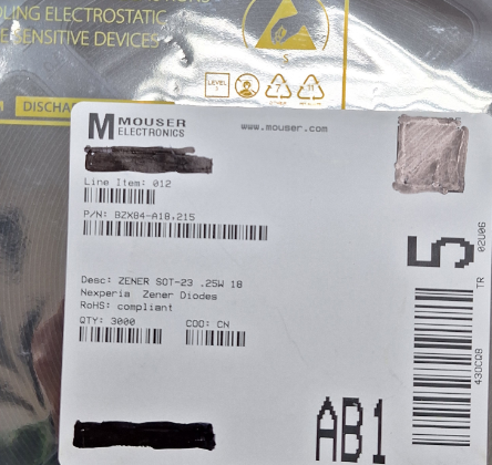
BZX84-A18,215 COUNTRY OF ORIGIN
|
BZX84-A18,215 PARAMETRIC INFO
|
BZX84-A18,215 PACKAGE INFO
|
BZX84-A18,215 MANUFACTURING INFO
|
BZX84-A18,215 PACKAGING INFO
|
BZX84-A18,215 APPLICATIONS
|
|
COUNTRY OF ORIGIN
|
China
|
|
PARAMETRIC INFO
|
| Type |
Voltage Regulator |
| Configuration |
Single |
| Typical Zener Voltage (V) |
18 |
| Polarity |
No |
| Maximum Reverse Leakage Current (uA) |
0.05 |
| Maximum Zener Impedance (Ohm) |
45 |
| Maximum Power Dissipation @ 25C (mW) |
250 |
| Maximum Power Dissipation (mW) |
250 |
| Typical Voltage Temperature Coefficient |
14.2mV/K |
| Test Current (mA) |
5 |
| Maximum Zener Voltage (V) |
18.18 |
| Minimum Zener Voltage (V) |
17.82 |
| Maximum Forward Voltage (V) |
0.9 |
| Maximum Diode Capacitance (pF) |
70 |
| Average Rectified Forward Current (A) |
0.2 |
| Zener Voltage Tolerance |
1% |
| Minimum Operating Temperature (°C) |
-55 |
| Maximum Operating Temperature (°C) |
150 |
|
|
PACKAGE INFO
|
| Supplier Package |
SOT-23 |
| Basic Package Type |
Lead-Frame SMT |
| Pin Count |
3 |
| Lead Shape |
Gull-wing |
| PCB |
3 |
| Tab |
N/R |
| Pin Pitch (mm) |
0.95 |
| Package Length (mm) |
3(Max) |
| Package Width (mm) |
1.4(Max) |
| Package Height (mm) |
1(Max) |
| Package Diameter (mm) |
N/R |
| Package Overall Length (mm) |
3(Max) |
| Package Overall Width (mm) |
2.5(Max) |
| Package Overall Height (mm) |
1.1(Max) |
| Seated Plane Height (mm) |
1.1(Max) |
| Mounting |
Surface Mount |
| Terminal Width (mm) |
0.48(Max) |
| Package Weight (g) |
N/A |
| Package Material |
Plastic |
| Package Description |
Small Outline Transistor |
| Package Family Name |
SOT |
| Jedec |
TO-236AB |
| Package Outline |
Link to Datasheet |
| Maximum PACKAGE_DIMENSION_L |
3 |
| Minimum PACKAGE_DIMENSION_L |
2.8 |
| Maximum PACKAGE_DIMENSION_W |
1.4 |
| Minimum PACKAGE_DIMENSION_W |
1.2 |
| Maximum Diameter |
N/R |
| Minimum Diameter |
N/R |
| Minimum Seated_Plane_Height |
0.9 |
| Minimum PACKAGE_DIMENSION_H |
N/A |
| Maximum PACKAGE_DIMENSION_H |
1 |
| Maximum Seated_Plane_Height |
1.1 |
|
|
MANUFACTURING INFO
|
| MSL |
1 |
| Maximum Reflow Temperature (°C) |
260 |
| Reflow Solder Time (Sec) |
30 |
| Number of Reflow Cycle |
3 |
| Standard |
N/A |
| Maximum Wave Temperature (°C) |
260 |
| Wave Solder Time (Sec) |
10 |
| Lead Finish(Plating) |
Sn |
| Under Plating Material |
CuAg |
| Terminal Base Material |
FeNi Alloy |
| Number of Wave Cycles |
1 |
|
|
PACKAGING INFO
|
| Packaging Suffix |
215 |
| Packaging |
Tape and Reel |
| Quantity Of Packaging |
3000 |
| Packaging Document |
Link to Datasheet |
|
|
| APPLICATIONS |
| • General regulation functions |
| |