 |
|
• Propagation delay time= 60 ns(typ)atCL =50 PF, VDD= 10V
|
| • Buffered inputs and outputs |
| • Standardized symmetrical output characteristics |
| • 100% tested for maximum quiescent current at 20V |
| • 5-V. 10.V, and 15-V parametric ratings |
| • Maximum input current of 1 μA at 18 Vover full package-temperature range:100 NA at 18 V and 25°c |
•Noise margin (over full package temperature)
1 Vat VDD=5V
2 Vat VDD= 10V
2.5 Vat VDD=15V |
| • Meets all requirements of JEDEC TentativeStandard No, 13B, "standard Speclfleatlonsfor Description of"B"Series CMOS Devic" |
|
| CATALOG |
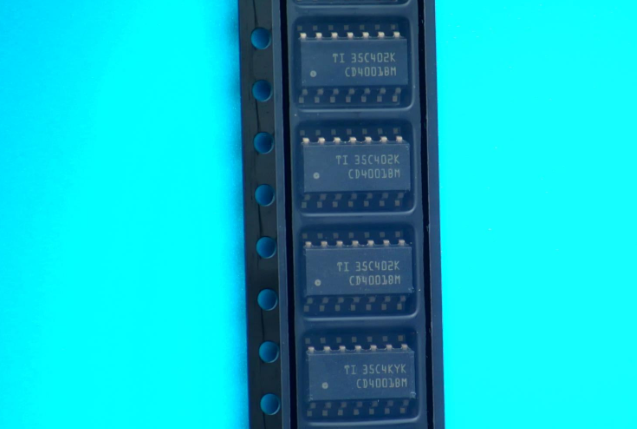
| CD4001BM96 COUNTRY OF ORIGIN |
| CD4001BM96 PARAMETRIC INFO |
| CD4001BM96 PACKAGE INFO |
| CD4001BM96 MANUFACTURING INFO |
| CD4001BM96 PACKAGING INFO |
|
| COUNTRY OF ORIGIN |
| Malaysia |
|
| PARAMETRIC INFO |
| Logic Family |
CD4000 |
| Logic Function |
NOR |
| Number of Element Inputs |
2-IN |
| Number of Element Outputs |
1 |
| Number of Elements per Chip |
4 |
| Number of Output Enables per Element |
0 |
| Number of Selection Inputs per Element |
0 |
| Output Type |
Push-Pull |
| Process Technology |
CMOS |
| Minimum Operating Supply Voltage (V) |
3 |
| Maximum Operating Supply Voltage (V) |
18 |
| Typical Operating Supply Voltage (V) |
3.3|5|9|12|15 |
| Maximum High Level Output Current (mA) |
-4.2(Min) |
| Maximum Low Level Output Current (mA) |
4.2(Min) |
| Minimum Operating Temperature (°C) |
-55 |
| Maximum Operating Temperature (°C) |
125 |
| Supplier Temperature Grade |
Military |
| Maximum Propagation Delay Time @ Maximum CL (ns) |
250@5V|120@10V|90@15V |
| Absolute Propagation Delay Time (ns) |
250 |
| Propagation Delay Test Condition (pF) |
50 |
| Maximum Quiescent Current (uA) |
5 |
| Typical Quiescent Current (uA) |
0.02 |
|
| PACKAGE INFO |
| Supplier Package |
SOIC |
| Basic Package Type |
Lead-Frame SMT |
| Pin Count |
14 |
| Lead Shape |
Gull-wing |
| PCB |
14 |
| Tab |
N/R |
| Pin Pitch (mm) |
1.27 |
| Package Length (mm) |
8.75(Max) |
| Package Width (mm) |
4(Max) |
| Package Height (mm) |
1.5(Max) |
| Package Diameter (mm) |
N/R |
| Package Overall Length (mm) |
8.75(Max) |
| Package Overall Width (mm) |
6.2(Max) |
| Package Overall Height (mm) |
1.75(Max) |
| Seated Plane Height (mm) |
1.75(Max) |
| Mounting |
Surface Mount |
| Package Weight (g) |
N/A |
| Package Material |
Plastic |
| Package Description |
Small Outline IC |
| Package Family Name |
SO |
| Jedec |
MS-012AB |
| Package Outline |
Link to Datasheet |
|
| MANUFACTURING INFO |
| MSL |
1 |
| Maximum Reflow Temperature (°C) |
260 |
| Reflow Solder Time (Sec) |
30 |
| Number of Reflow Cycle |
3 |
| Standard |
J-STD-020D |
| Reflow Temp. Source |
Link to Datasheet |
| Maximum Wave Temperature (°C) |
N/R |
| Wave Solder Time (Sec) |
N/R |
| Lead Finish(Plating) |
Au |
| Under Plating Material |
Pd over Ni |
| Terminal Base Material |
Cu Alloy |
|
| PACKAGING INFO |
| Packaging Suffix |
96 |
| Packaging |
Tape and Reel |
| Quantity Of Packaging |
2500 |
| Reel Diameter (in) |
13 |
| Tape Pitch (mm) |
8 |
| Tape Width (mm) |
16 |
| Component Orientation |
Q1 |
| Packaging Document |
Link to Datasheet |
|