|
| |
• Wide range of digital and analog signal levels:– Digital: 3 V to 20 V– Analog: ≤ 20 VP-P
|
• Low ON resistance, 125 Ω (typical) over 15 VP-P signal input range for VDD – VEE = 18 V
|
• High OFF resistance, channel leakage of ±100 pA (typical) at VDD – VEE = 18 V
|
• Logic-level conversion for digital addressing signals of 3 V to 20 V (VDD – VSS = 3 V to 20V) to switch analog signals to 20 VP-P (VDD – VEE
= 20 V) matched switch characteristics, rON = 5 Ω(typical) for VDD – VEE = 15 V very low quiescent power dissipation under all digital-control input and supply conditions, 0.2 µW (typical) at VDD – VSS = VDD – VEE = 10 V |
| • Binary address decoding on chip |
| • 5 V, 10 V, and 15 V parametric ratings |
| • 100% tested for quiescent current at 20 V |
| • Maximum input current of 1 µA at 18 V over full package temperature range, 100 nA at 18 V and 25°C |
| • Break-before-make switching eliminates channel overlap |
| |
| CATALOG |
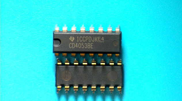
| CD4053BE COUNTRY OF ORIGIN |
CD4053BE PARAMETRIC INFO
|
CD4053BE PACKAGE INFO
|
CD4053BE MANUFACTURING INFO
|
CD4053BE PACKAGING INFO
|
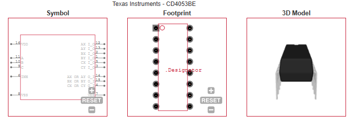
CD4053BE EACD MODELS
|
| CD4053BE APPLICATIONS |
|
| COUNTRY OF ORIGIN |
| Mexico |
| Malaysia |
| China |
| |
PARAMETRIC INFO
|
| Type |
Analog Multiplexer |
| Number of Channels per Chip |
3 |
| Multiplexer Architecture |
2:1 |
| Maximum On Resistance Range (Ohm) |
>=1000 |
| Configuration |
Triple 2:1 |
| Number of Inputs per Chip |
6 |
| Function |
General |
| Process Technology |
CMOS |
| Logic Family |
CD4000 |
| Number of Outputs per Chip |
3 |
| Chip Enable Signals |
Yes |
| Maximum On Resistance (Ohm) |
1050@5V |
| Maximum Propagation Delay Bus to Bus (ns) |
20@15V|30@10V|60@5V |
| Maximum Turn-On Time (ns) |
720@5V |
| Maximum Turn-Off Time (ns) |
450@5V |
| Input Signal Type |
Single |
| Output Signal Type |
Single |
| Propagation Delay Test Condition (pF) |
50 |
| Maximum Frequency (25°C) @ Vcc (MHz) |
60(Typ)@10V|30(Typ)@10V |
| Special Features |
Break-Before-Make |
| Minimum Operating Temperature (°C) |
-55 |
| Maximum Operating Temperature (°C) |
125 |
| Maximum Storage Temperature (°C) |
150 |
| Minimum Storage Temperature (°C) |
-65 |
| Power Supply Type |
Single|Dual |
| Minimum Single Supply Voltage (V) |
3 |
| Typical Single Supply Voltage (V) |
5|12|16 |
| Maximum Single Supply Voltage (V) |
20 |
| Typical Dual Supply Voltage (V) |
±2.5|±5|±10 |
|
|
PACKAGE INFO
|
| Supplier Package |
PDIP |
| Basic Package Type |
Through Hole |
| Pin Count |
16 |
| Lead Shape |
Through Hole |
| PCB |
16 |
| Tab |
N/R |
| Pin Pitch (mm) |
2.54 |
| Package Length (mm) |
19.69(Max) |
| Package Width (mm) |
6.6(Max) |
| Package Height (mm) |
5.08(Max) - 0.51(Min) |
| Package Diameter (mm) |
N/R |
| Package Overall Length (mm) |
19.69(Max) |
| Package Overall Width (mm) |
10.92(Max) |
| Package Overall Height (mm) |
5.08(Max) |
| Seated Plane Height (mm) |
5.08(Max) |
| Mounting |
Through Hole |
| Package Weight (g) |
N/A |
| Package Material |
Plastic |
| Package Description |
Plastic Dual In Line Package |
| Package Family Name |
DIP |
| Jedec |
MS-001BB |
| Package Outline |
Link to Datasheet |
|
|
MANUFACTURING INFO
|
| MSL |
N/R |
| Maximum Reflow Temperature (°C) |
N/R |
| Reflow Solder Time (Sec) |
N/R |
| Maximum Wave Temperature (°C) |
N/A |
| Wave Solder Time (Sec) |
N/A |
| Wave Temp. Source |
Link to Datasheet |
| Lead Finish(Plating) |
Au |
| Under Plating Material |
Pd over Ni |
| Terminal Base Material |
Cu Alloy |
|
|
PACKAGING INFO
|
| Packaging |
Tube |
| Quantity Of Packaging |
25 |
| Packaging Document |
Link to Datasheet |
|
|
ECAD MODELS
|
|
| APPLICATIONS |
| • Analog and digital multiplexing and demultiplexing |
| • Analog to digital and digital to analog conversion |
| • Signal gating |
| • Factory automation |
| • Televisions |
| • Appliances |
| • Consumer audio |
| • Programmable logic circuits |
| • Sensors |
| |