 |
|
| ■ Schmitt-trigger action on each input with no external components |
| ■ Hysteresis voltage typically 0.9 V at VDD=5 V and 2.3 V at VDD=10 V |
| ■ Noise immunity greater than 50% |
| ■ No limit on input rise and fall timreS |
| ■ Standardized, symmetrical output characteristics |
| ■ 100% tested for quiescent current at 20 V |
| ■ Maximum input current of 1 μA at 18 V over full package-temperature range, 100 nA at 18 V and 25°℃ |
| ■ 5-V, 10-V, and 15-V parametric ratings |
|
■ Meets all requirements of JEDEC for Description of 'B' Series CMOS Devices"
|
|
| CATALOG |
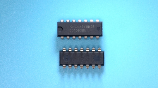
| CD4093BE COUNTRY OF ORIGIN |
| CD4093BE PARAMETRIC INFO |
| CD4093BE PACKAGE INFO |
| CD4093BE MANUFACTURING INFO |
| CD4093BE PACKAGING INFO |
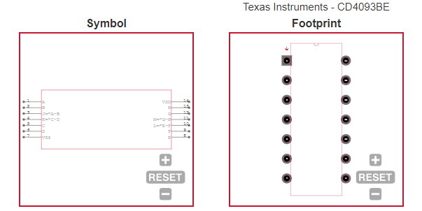
| CD4093BE ECAD MODELS |
| CD4093BE APPLICATIONS |
|
| COUNTRY OF ORIGIN |
| China |
| Thailand |
| Malaysia |
| Mexico |
|
| PARAMETRIC INFO |
| Logic Family |
CD4000 |
| Logic Function |
NAND |
| Number of Element Inputs |
2-IN |
| Number of Element Outputs |
1 |
| Number of Elements per Chip |
4 |
| Number of Output Enables per Element |
0 |
| Number of Selection Inputs per Element |
0 |
| Output Type |
Push-Pull |
| Process Technology |
CMOS |
| Input Type |
Schmitt Trigger |
| Minimum Operating Supply Voltage (V) |
3 |
| Maximum Operating Supply Voltage (V) |
18 |
| Typical Operating Supply Voltage (V) |
3.3|5|9|12|15 |
| Maximum High Level Output Current (mA) |
-4.2(Min) |
| Maximum Low Level Output Current (mA) |
4.2(Min) |
| Minimum Operating Temperature (°C) |
-55 |
| Maximum Operating Temperature (°C) |
125 |
| Maximum Propagation Delay Time @ Maximum CL (ns) |
380@5V|180@10V|130@15V |
| Absolute Propagation Delay Time (ns) |
380 |
| Propagation Delay Test Condition (pF) |
50 |
| Maximum Quiescent Current (uA) |
20 |
| Typical Quiescent Current (uA) |
0.04 |
|
| |
| PACKAGE INFO |
| Supplier Package |
PDIP |
| Basic Package Type |
Through Hole |
| Pin Count |
14 |
| Lead Shape |
Through Hole |
| PCB |
14 |
| Tab |
N/R |
| Pin Pitch (mm) |
2.54 |
| Package Length (mm) |
19.69(Max) |
| Package Width (mm) |
6.6(Max) |
| Package Height (mm) |
5.08(Max) - 0.51(Min) |
| Package Diameter (mm) |
N/R |
| Package Overall Length (mm) |
19.69(Max) |
| Package Overall Width (mm) |
10.92(Max) |
| Package Overall Height (mm) |
5.08(Max) |
| Seated Plane Height (mm) |
5.08(Max) |
| Mounting |
Through Hole |
| Package Weight (g) |
N/A |
| Package Material |
Plastic |
| Package Description |
Plastic Dual In Line Package |
| Package Family Name |
DIP |
| Jedec |
MS-001AA |
| Package Outline |
Link to Datasheet |
|
| |
| MANUFACTURING INFO |
| MSL |
N/R |
| Maximum Reflow Temperature (°C) |
N/R |
| Reflow Solder Time (Sec) |
N/R |
| Number of Reflow Cycle |
N/R |
| Maximum Wave Temperature (°C) |
N/A |
| Wave Solder Time (Sec) |
N/A |
| Wave Temp. Source |
Link to Datasheet |
| Lead Finish(Plating) |
Au |
| Under Plating Material |
Pd over Ni |
| Terminal Base Material |
Cu Alloy |
| Shelf Life Period |
5 Years |
| Shelf Life Condition |
N/A |
|
| |
| PACKAGING INFO |
| Packaging |
Tube |
| Quantity Of Packaging |
25 |
| Packaging Document |
Link to Datasheet |
|
| |
| ECAD MODELS |
 |
|
| APPLICATIONS |
| ■ Wave and pulse shapers |
| ■ High-noise-environment systems |
| ■ Monostable multivibrators |
| ■ Astable multivibrators |
| ■ NAND logic |
| |
|