 |
|
| • Wide Analog Input Voltage Range |
• Low “ON” Resistance
- VCC = 4.5V. . . . . . . . . . . . . . . . . . . . . . . . . . . 70Ω(Typ)
- VCC = 6V . . . . . . . . . . . . . . . . . . . . . . . . . . . . 60Ω(Typ) |
| • Fast Switching and Propagation Speeds |
| • “Break-Before-Make” Switching. . . . . 6ns (Typ) at 4.5V |
| • Available in Both Narrow and Wide-Body Plastic
Packages |
• Fanout (Over Temperature Range)
- Standard Outputs . . . . . . . . . . . . . . . 10 LSTTL Loads
- Bus Driver Outputs . . . . . . . . . . . . . 15 LSTTL Loads
|
| • Wide Operating Temperature Range . . . -55oC to 125oC |
| • Balanced Propagation Delay and Transition Times |
| • Significant Power Reduction Compared to LSTTL
Logic ICs |
• HC Types
- 2V to 6V Operation
- High Noise Immunity: NIL = 30%, NIH = 30% of VCC
at VCC = 5V |
• HCT Types
- 4.5V to 5.5V Operation
- Direct LSTTL Input Logic Compatibility,
VIL= 0.8V (Max), VIH = 2V (Min)
- CMOS Input Compatibility, Il ≤ 1µA at VOL, VOH
|
|
| CATALOG |
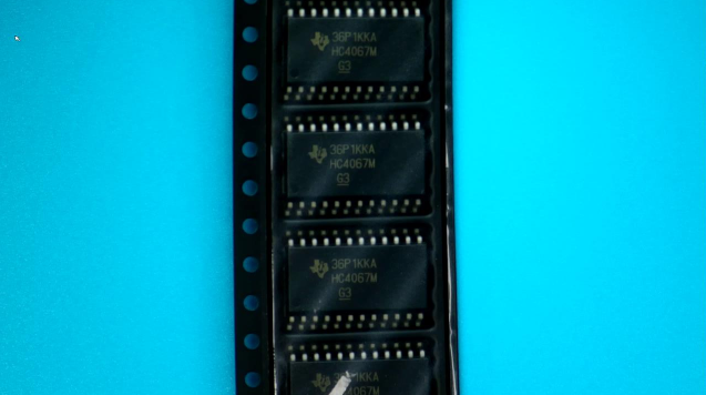
| CD74HC4067M96 COUNTRY OF ORIGIN |
| CD74HC4067M96 PARAMETRIC INFO |
| CD74HC4067M96 PACKAGE INFO |
| CD74HC4067M96 MANUFACTURING INFO |
| CD74HC4067M96 PACKAGING INFO |
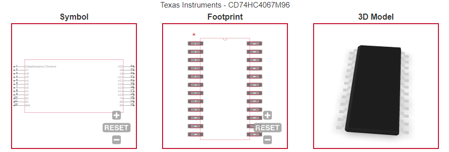
| CD74HC4067M96 ECAD MODELS |
|
| COUNTRY OF ORIGIN |
| China |
| Malaysia |
| Taiwan (Province of China) |
|
| PARAMETRIC INFO |
| Type |
Analog Multiplexer |
| Number of Channels per Chip |
1 |
| Multiplexer Architecture |
16:1 |
| Maximum On Resistance Range (Ohm) |
150 to 250 |
| Configuration |
Single 16:1 |
| Number of Inputs per Chip |
16 |
| Function |
General |
| Process Technology |
CMOS |
| Number of Outputs per Chip |
1 |
| Logic Family |
HC |
| Chip Enable Signals |
Yes |
| Maximum On Resistance (Ohm) |
180@4.5V |
| Maximum Propagation Delay Bus to Bus (ns) |
13@6V|15@4.5V|75@2V |
| Maximum Turn-On Time (ns) |
300@2V |
| Maximum Turn-Off Time (ns) |
290@2V |
| Input Signal Type |
Single |
| Output Signal Type |
Single |
| Propagation Delay Test Condition (pF) |
50 |
| Maximum Low Level Output Current (mA) |
25 |
| Maximum High Level Output Current (mA) |
25 |
| Maximum Frequency (25°C) @ Vcc (MHz) |
89@4.5V |
| Special Features |
Break-Before-Make |
| Minimum Operating Temperature (°C) |
-55 |
| Maximum Operating Temperature (°C) |
125 |
| Power Supply Type |
Single |
| Minimum Single Supply Voltage (V) |
2 |
| Typical Single Supply Voltage (V) |
3|5 |
| Maximum Single Supply Voltage (V) |
6 |
|
| |
| PACKAGE INFO |
| Supplier Package |
SOIC |
| Basic Package Type |
Lead-Frame SMT |
| Pin Count |
24 |
| Lead Shape |
Gull-wing |
| PCB |
24 |
| Tab |
N/R |
| Pin Pitch (mm) |
1.27 |
| Package Length (mm) |
15.6(Max) |
| Package Width (mm) |
7.6(Max) |
| Package Height (mm) |
2.35(Max) |
| Package Diameter (mm) |
N/R |
| Package Overall Length (mm) |
15.6(Max) |
| Package Overall Width (mm) |
10.63(Max) |
| Package Overall Height (mm) |
2.65(Max) |
| Seated Plane Height (mm) |
2.65(Max) |
| Mounting |
Surface Mount |
| Package Weight (g) |
N/A |
| Package Material |
Plastic |
| Package Description |
Small Outline IC |
| Package Family Name |
SO |
| Jedec |
MS-013AD |
| Package Outline |
Link to Datasheet |
|
| |
| MANUFACTURING INFO |
| MSL |
1 |
| Maximum Reflow Temperature (°C) |
260 |
| Reflow Solder Time (Sec) |
30 |
| Number of Reflow Cycle |
3 |
| Standard |
J-STD-020D |
| Reflow Temp. Source |
Link to Datasheet |
| Maximum Wave Temperature (°C) |
N/R |
| Wave Solder Time (Sec) |
N/R |
| Lead Finish(Plating) |
Matte Sn|Au |
| Under Plating Material |
N/A|Pd over Ni |
| Terminal Base Material |
Cu Alloy |
|
| |
| PACKAGING INFO |
| Packaging Suffix |
96 |
| Packaging |
Tape and Reel |
| Quantity Of Packaging |
2000 |
| Reel Diameter (in) |
13 |
| Tape Pitch (mm) |
12 |
| Tape Width (mm) |
24 |
| Component Orientation |
Q1 |
| Packaging Document |
Link to Datasheet |
|
| |
| ECAD MODELS |
 |
|