|
|
• Performance– INL: ±1 LSB Maximum at 16-Bit Resolution– TUE: ±0.1% of FSR Maximum
|
• Integrated 2.5 V Precision Internal Reference– Initial Accuracy: ±5 mV Maximum– Low Drift: 2 ppm/°C Typical, DAC80508
|
• High Drive Capability: 20 mA with 0.5 V from Supply Rails
|
| • Flexible Output Configuration– User Selectable Gain: 2, 1 or ½– Reset to Zero Scale or Midscale– Clear Output Function: DACx0508C
|
| • Wide Operating Range– Power Supply: 2.7 V to 5.5 V– Temperature Range: –40˚C to 125˚C |
| • 50 MHz SPI Compatible Serial Interface– 1.7 V to 5.5 V Operation– Daisy Chain Operation– CRC Error Check |
| • Low Power: 0.6 mA/Channel at 5.5 V |
| • Small Packages:– 3 mm × 3 mm, 16-Pin WQFN– 2.4 mm x 2.4 mm, 16-Pin DSBGA |
|
| CATALOG |
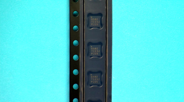
| DAC60508ZRTET COUNTRY OF ORIGIN |
DAC60508ZRTET PARAMETRIC INFO
|
DAC60508ZRTET PACKAGE INFO
|
DAC60508ZRTET MANUFACTURING INFO
|
DAC60508ZRTET PACKAGING INFO
|
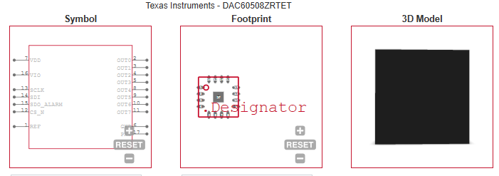
DAC60508ZRTET ECAD MODELS
|
| DAC60508ZRTET APPLICATIONS |
|
| COUNTRY OF ORIGIN |
| Malaysia |
| Thailand |
|
PARAMETRIC INFO
|
| Architecture |
R-2R |
| Resolution |
12bit |
| Number of DAC Channels |
8 |
| Number of Outputs per Chip |
8 |
| Conversion Rate |
1Msps |
| Converter Type |
General Purpose |
| Input Code |
Straight Binary |
| Typical Settling Time (us) |
5 |
| Maximum Analog Output Voltage |
6.3V |
| Minimum Analog Output Voltage |
-0.3V |
| Multiplying Function |
yes |
| Output Type |
Voltage |
| Voltage Reference |
Internal|External |
| Digital Interface Type |
Serial (4-Wire, SPI) |
| Output Polarity |
Bipolar |
| Integral Nonlinearity Error |
±1LSB |
| Full Scale Error |
±0.22%FSR |
| Minimum Operating Temperature (°C) |
-40 |
| Maximum Operating Temperature (°C) |
125 |
| Minimum Storage Temperature (°C) |
-60 |
| Maximum Storage Temperature (°C) |
150 |
| Power Supply Type |
Single |
| Minimum Single Supply Voltage (V) |
2.7 |
| Typical Single Supply Voltage (V) |
3.3|5 |
| Maximum Single Supply Voltage (V) |
5.5 |
| Digital Supply Support |
no |
|
|
PACKAGE INFO
|
| Supplier packaging |
WQF |
| Basic package type |
Non-Lead-Frame SMT |
| Number of pins |
16 |
| Pin shape |
No Lead |
| PCB |
16 |
| ears |
N/R |
| Pin spacing (mm) |
0.5 |
| Package length (mm) |
3.15(Max) |
| Package width (mm) |
3.15(Max) |
| Package height (mm) |
0.75(Max) |
| Package diameter (mm) |
N/R |
| Package Overall Length (mm) |
3.15(Max) |
| Package Overall Width (mm) |
3.15(Max) |
| Package Overall Height (mm) |
0.8(Max) |
| Mounting surface height (mm) |
0.8(Max) |
| Install |
Surface Mount |
| Package weight (g) |
not applicable |
| Packaging materials |
Plastic |
| package instruction |
Very Very Thin Quad Flat No Lead Package, Exposed Pad |
| Package series name |
QFN |
| JEDEC |
not applicable |
|
|
MANUFACTURING INFO
|
| MSL |
2 |
| Maximum reflow temperature (°C) |
260 |
| Reflow soldering time (seconds) |
30 |
| Number of reflow cycles |
3 |
| standard |
J-STD-020D |
| Reflow temperature source |
Link to datasheet |
| Maximum wave soldering temperature (°C) |
N/R |
| Wave soldering time (seconds) |
N/R |
| Lead Finish(Plating) |
Au |
| Plating materials |
Pd over Ni |
| Terminal Base Material |
Cu Alloy |
|
|
PACKAGING INFO
|
| Packaging Suffix |
T |
| Package |
Tape and reel packaging |
| Packing quantity |
250 |
|
|
ECAD MODELS
|
|
|
APPLICATIONS
|
• Optical Networking
|
| • Wireless Infrastructure |
| • Industrial Automation |
• Data Acquisition Systems
|
| |
| |