 |
|
| • Low On-Resistance |
| • Low Input Capacitance |
| • Fast Switching Speed |
| • Low Input/Output Leakage |
| • ESD Protected Up To 3kV |
| • Totally Lead-Free & Fully RoHS Compliant (Notes 1 & 2)
|
| • Halogen and Antimony Free. “Green” Device (Note 3)
|
| • For automotive applications requiring specific change control
(i.e.: parts qualified to AEC-Q100/101/200, PPAP capable, and
manufactured in IATF 16949 certified facilities), please refer
to the related automotive grade (Q-suffix) part. A listing can
be found at |
| • This part is qualified to JEDEC standards (as references in
AEC-Q) for High Reliability. |
|
| CATALOG |
| DMP2100U-7 COUNTRY OF ORIGIN |
| DMP2100U-7 PARAMETRIC INFO |
| DMP2100U-7 PACKAGE INFO |
| DMP2100U-7 MANUFACTURING INFO |
| DMP2100U-7 PACKAGING INFO |
| DMP2100U-7 ECAD MODELS |
| DMP2100U-7 APPLICATIONS |
|
| COUNTRY OF ORIGIN |
| China |
|
| PARAMETRIC INFO |
| Channel Type |
P |
| Channel Mode |
Enhancement |
| Configuration |
Single |
| Maximum Drain Source Voltage (V) |
20 |
| Maximum Continuous Drain Current (A) |
4.3 |
| Maximum Gate Source Voltage (V) |
±10 |
| Maximum Drain Source Resistance (mOhm) |
38@10V |
| Typical Gate Charge @ Vgs (nC) |
9.1@4.5V |
| Maximum Power Dissipation (mW) |
1300 |
| Category |
Power MOSFET |
| Typical Input Capacitance @ Vds (pF) |
216@15V |
| Typical Turn-On Delay Time (ns) |
80 |
| Typical Turn-Off Delay Time (ns) |
688 |
| Typical Fall Time (ns) |
423 |
| Typical Rise Time (ns) |
155 |
| Maximum Gate Source Leakage Current (nA) |
10000 |
| Maximum Gate Threshold Voltage (V) |
1.4 |
| Maximum IDSS (uA) |
1 |
| Number of Elements per Chip |
1 |
| Minimum Storage Temperature (°C) |
-55 |
| Maximum Storage Temperature (°C) |
150 |
| Minimum Operating Temperature (°C) |
-55 |
| Maximum Operating Temperature (°C) |
150 |
|
| |
| PACKAGE INFO |
| Supplier Package |
SOT-23 |
| Basic Package Type |
Lead-Frame SMT |
| Pin Count |
3 |
| Lead Shape |
Gull-wing |
| PCB |
3 |
| Tab |
N/R |
| Pin Pitch (mm) |
0.92 |
| Package Length (mm) |
2.9 |
| Package Width (mm) |
1.3 |
| Package Height (mm) |
0.98 |
| Package Diameter (mm) |
N/R |
| Package Overall Length (mm) |
2.9 |
| Package Overall Width (mm) |
2.4 |
| Package Overall Height (mm) |
1.03 |
| Seated Plane Height (mm) |
1.03 |
| Mounting |
Surface Mount |
| Package Weight (g) |
N/A |
| Package Material |
Plastic |
| Package Description |
Small Outline Transistor |
| Package Family Name |
SOT |
| Jedec |
TO-236AA |
| Package Outline |
Link to Datasheet |
|
| |
| MANUFACTURING INFO |
| MSL |
1 |
| Maximum Reflow Temperature (°C) |
260 |
| Reflow Solder Time (Sec) |
30 |
| Number of Reflow Cycle |
3 |
| Standard |
J-STD-020D |
| Reflow Temp. Source |
Link to Datasheet |
| Maximum Wave Temperature (°C) |
N/R |
| Wave Solder Time (Sec) |
N/R |
| Lead Finish(Plating) |
Matte Sn annealed |
| Under Plating Material |
N/A |
| Terminal Base Material |
FeNi Alloy |
|
| |
| PACKAGING INFO |
| Packaging Suffix |
7 |
| Packaging |
Tape and Reel |
| Quantity Of Packaging |
3000 |
| Reel Diameter (in) |
7 |
| Reel Width (mm) |
8.4 |
| Tape Pitch (mm) |
4 |
| Tape Width (mm) |
8 |
| Feed Hole Pitch (mm) |
4 |
| Hole Center to Component Center (mm) |
2 |
| Component Orientation |
Single Pin At Sprocket Hole |
| Packaging Document |
Link to Datasheet |
| Tape Type |
Embossed |
|
| |
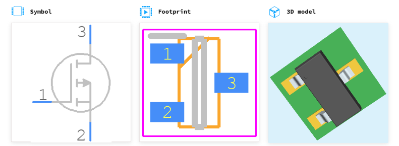
| ECAD MODELS |
 |
|
| APPLICATIONS |
| • Load Switch |
| • Power Management Functions |
| |
|