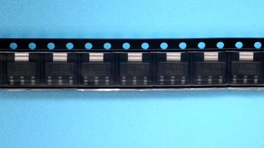
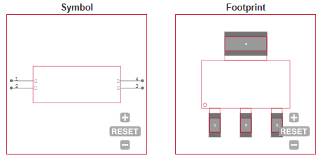
DMP6250SE-13 Diodes Incorporated MOSFET P-CH 60V 2.1A SOT223

label:
2024/10/16 151
DMP6250SE-13 Diodes Incorporated MOSFET P-CH 60V 2.1A SOT223


• Low Gate Drive
• Low Input Capacitance
• Fast Switching Speed
• Totally Lead-Free & Fully RoHS Compliant (Notes 1 & 2)
• Halogen and Antimony Free. “Green” Device (Note 3)
• Qualified to AEC-Q101 Standards for High Reliability


CATALOG
DMP6250SE-13 COUNTRY OF ORIGIN
DMP6250SE-13 PARAMETRIC INFO
DMP6250SE-13 PACKAGE INFO
DMP6250SE-13 MANUFACTURING INFO
DMP6250SE-13 PACKAGING INFO
DMP6250SE-13 ECAD MODELS
DMP6250SE-13 APPLICATIONS


COUNTRY OF ORIGIN
China


PARAMETRIC INFO
Channel Type P
Channel Mode Enhancement
Configuration Single Dual Drain
Maximum Drain Source Voltage (V) 60
Maximum Absolute Continuous Drain Current (A) 6.1
Maximum Continuous Drain Current (A) 2.1
Maximum Gate Source Voltage (V) ±20
Maximum Drain Source Resistance (mOhm) 250@10V
Typical Gate Charge @ Vgs (nC) 4.8@4.5V|9.7@10V
Typical Gate Charge @ 10V (nC) 9.7
Maximum Power Dissipation (mW) 1800
Category Power MOSFET
Typical Input Capacitance @ Vds (pF) 551@30V
Typical Turn-On Delay Time (ns) 6.3
Typical Turn-Off Delay Time (ns) 91.4
Typical Fall Time (ns) 39.8
Typical Rise Time (ns) 10.3
Maximum Gate Source Leakage Current (nA) 100
Maximum Gate Threshold Voltage (V) 3
Maximum IDSS (uA) 1
Number of Elements per Chip 1
Minimum Storage Temperature (°C) -55
Maximum Storage Temperature (°C) 150
Minimum Operating Temperature (°C) -55
Maximum Operating Temperature (°C) 150

 
PACKAGE INFO
Supplier Package SOT-223
Basic Package Type Lead-Frame SMT
Pin Count 4
Lead Shape Gull-wing
PCB 3
Tab Tab
Pin Pitch (mm) 2.3
Package Length (mm) 6.5
Package Width (mm) 3.5
Package Height (mm) 1.6
Package Diameter (mm) N/R
Package Overall Length (mm) 6.5
Package Overall Width (mm) 7
Package Overall Height (mm) 1.65
Seated Plane Height (mm) 1.65
Mounting Surface Mount
Package Weight (g) N/A
Package Material Plastic
Package Description Small Outline Transistor
Package Family Name SOT
Jedec TO-261AA
Package Outline Link to Datasheet


MANUFACTURING INFO
MSL 1
Maximum Reflow Temperature (°C) 260
Reflow Solder Time (Sec) 30
Number of Reflow Cycle 3
Standard J-STD-020D
Reflow Temp. Source Link to Datasheet
Maximum Wave Temperature (°C) N/R
Wave Solder Time (Sec) N/R
Lead Finish(Plating) Matte Sn annealed
Under Plating Material N/A
Terminal Base Material Cu


PACKAGING INFO
Packaging Suffix 13
Packaging Tape and Reel
Quantity Of Packaging 2500
Reel Diameter (in) 13
Reel Width (mm) 12.4
Tape Pitch (mm) 8
Tape Width (mm) 12
Feed Hole Pitch (mm) 4
Hole Center to Component Center (mm) 2
Component Orientation Tab At Sprocket Hole
Packaging Document Link to Datasheet
Tape Type Embossed


ECAD MODELS


APPLICATIONS
• Motor Control
• DC-DC Converters
• Power Management Functions
• Uninterrupted Power Supply
Продукт RFQ