|
| |
• Rated to +175°C – Ideal for High Ambient Temperature Environments
|
• 100% Unclamped Inductive Switching – Ensures More Reliable and Robust End Application
|
• Low Qg – Minimizes Switching Loss
|
| • Low RDS(ON) – Minimizes On State Loss
|
| • Lead-Free Finish; RoHS Compliant (Notes 1 & 2) |
| • Halogen and Antimony Free. “Green” Device (Note 3) |
| • Qualified to AEC-Q101 Standards for High Reliability |
| • An Automotive-Compliant Part is Available Under Separate Datasheet (DMPH6050SK3Q) |
|
| CATALOG |
| DMPH6050SK3-13 COUNTRY OF ORIGIN |
DMPH6050SK3-13 PARAMETRIC INFO
|
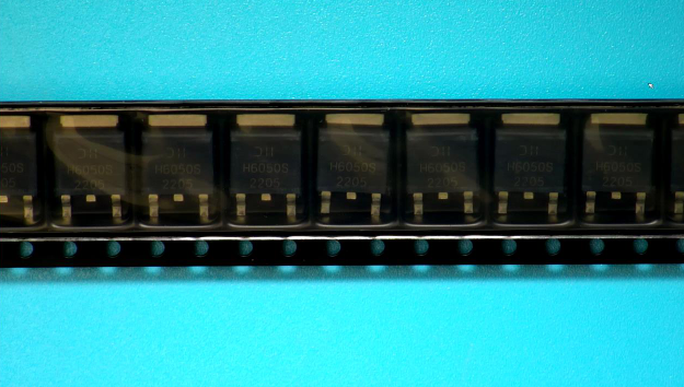
DMPH6050SK3-13 PACKAGE INFO
|
DMPH6050SK3-13 MANUFACTURING INFO
|
DMPH6050SK3-13 PACKAGING INFO
|
| DMPH6050SK3-13 APPLICATIONS |
|
| COUNTRY OF ORIGIN |
| China |
|
PARAMETRIC INFO
|
| Channel Type |
P |
| Configuration |
Single |
| Channel Mode |
Enhancement |
| Maximum Drain Source Voltage (V) |
60 |
| Maximum Continuous Drain Current (A) |
7.2 |
| Maximum Absolute Continuous Drain Current (A) |
23.6 |
| Maximum Gate Source Voltage (V) |
±20 |
| Maximum Drain Source Resistance (mOhm) |
50@10V |
| Typical Gate Charge @ Vgs (nC) |
25@10V|12@4.5V |
| Typical Gate Charge @ 10V (nC) |
25 |
| Maximum Power Dissipation (mW) |
3800 |
| Category |
Power MOSFET |
| Typical Input Capacity @ Vds (pF) |
1377@30V |
| Typical Turn-On Delay Time (ns) |
5.3 |
| Typical Turn-Off Delay Time (ns) |
49.4 |
| Typical Fall Time (ns) |
29.7 |
| Typical Rise Time (ns) |
8.6 |
| Maximum Gate Source Leakage Current (nA) |
100 |
| Maximum Gate Threshold Voltage (V) |
3 |
| Maximum IDSS (uA) |
1 |
| Number of Elements per Chip |
1 |
| Minimum Storage Temperature (°C) |
-55 |
| Maximum Storage Temperature (°C) |
175 |
| Minimum Operating Temperature (°C) |
-55 |
| Maximum Operating Temperature (°C) |
175 |
| Supplier Temperature Rating |
car |
|
|
PACKAGE INFO
|
| Supplier packaging |
DPAK |
| Number of pins |
3 |
| PCB |
2 |
| ears |
ears |
| Package length (mm) |
6.58 |
| Package width (mm) |
6.1 |
| Package height (mm) |
2.29 |
| Package diameter (mm) |
N/R |
| Install |
Surface Mount |
| package instruction |
Deca Watt Package |
| Package series name |
TO-252 |
| Package outline |
Link to datasheet |
|
|
MANUFACTURING INFO
|
| Maximum reflow temperature (°C) |
260 |
| Reflow soldering time (seconds) |
30 |
| Number of reflow cycles |
3 |
| standard |
J-STD-020D |
| Reflow temperature source |
Link to datasheet |
| Maximum wave soldering temperature (°C) |
N/R |
| Lead Finish(Plating) |
Matte Sn annealed |
|
|
PACKAGING INFO
|
| Packaging Suffix |
13 |
| Package |
Tape and reel packaging |
| Packing quantity |
2500 |
| packaging type file |
Link to datasheet |
|
|
| APPLICATIONS |
| • Load Switch |
| • DC-DC Converters |
| • Motor Driving |
| |