|
| |
• Very low VF
|
• Extremely low switching losses
|
• Low IRM values
|
| • Improved thermal behavior |
| • High reliability circuit operation |
| • Low voltage peaks for reduced protection circuits |
| • Low noise switching |
| • Terminals finish: 100% Pure Tin |
| • This is a Pb-free device |
| • Epoxy meets UL 94V-0 |
| |
| CATALOG |
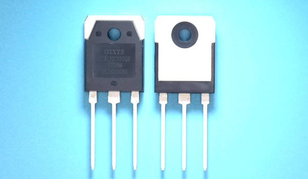
| DSA120C150QB COUNTRY OF ORIGIN |
DSA120C150QB PARAMETRIC INFO
|
DSA120C150QB PACKAGE INFO
|
DSA120C150QB MANUFACTURING INFO
|
| DSA120C150QB APPLICATIONS |
|
| COUNTRY OF ORIGIN |
| Korea (Republic of) |
|
PARAMETRIC INFO
|
| Type |
Schottky Diode |
| Configuration |
Dual Common Cathode |
| Maximum DC Reverse Voltage (V) |
150 |
| Peak Reverse Repetitive Voltage (V) |
150 |
| Maximum Continuous Forward Current (A) |
120 |
| Maximum Power Dissipation (mW) |
375000 |
| Peak Forward Voltage (V) |
0.93@60A |
| Peak Non-Repetitive Surge Current (A) |
800 |
| Peak Reverse Current (uA) |
900 |
| Operating Junction Temperature (°C) |
-55 to 175 |
| Minimum Storage Temperature (°C) |
-55 |
| Maximum Storage Temperature (°C) |
150 |
| Minimum Operating Temperature (°C) |
-55 |
| Maximum Operating Temperature (°C) |
150 |
|
|
PACKAGE INFO
|
| Supplier Package |
TO-3P |
| Basic Package Type |
Through Hole |
| Pin Count |
3 |
| Lead Shape |
Through Hole |
| PCB |
3 |
| Tab |
Tab |
| Pin Pitch (mm) |
5.45 |
| Package Length (mm) |
15.8(Max) |
| Package Width (mm) |
4.9(Max) |
| Package Height (mm) |
N/A |
| Package Diameter (mm) |
N/R |
| Seated Plane Height (mm) |
23.9(Max) |
| Mounting |
Through Hole |
| Package Material |
Plastic |
| Package Description |
Transistor Outline Package |
| Package Family Name |
TO |
| Jedec |
N/A |
| Package Outline |
Link to Datasheet |
|
|
MANUFACTURING INFO
|
| MSL |
N/R |
| Maximum Reflow Temperature (°C) |
N/R |
| Reflow Solder Time (Sec) |
N/R |
| Maximum Wave Temperature (°C) |
N/A |
| Wave Solder Time (Sec) |
N/A |
| Wave Temp. Source |
Link to Datasheet |
| Lead Finish(Plating) |
Sn |
| Under Plating Material |
N/A |
| Terminal Base Material |
N/A |
|
|
| APPLICATIONS |
| • Rectifiers in switch mode power supplies (SMPS)
|
| • Free wheeling diode in low voltage converters |
|
| |