 |
||||||||||||||||||||||||||||||||||||||||||||||||||||||||||||||||||||||||||||||||||||||
| |
||||||||||||||||||||||||||||||||||||||||||||||||||||||||||||||||||||||||||||||||||||||
| ■ High-density architecture with 4,608 to 68,416 LEs ● M4K embedded memory blocks ● Up to 1.1 Mbits of RAM available without reducing available logic ● 4,096 memory bits per block (4,608 bits per block including 512 parity bits) ● Variable port configurations of ×1, ×2, ×4, ×8, ×9, ×16, ×18, ×32, and ×36 ● True dual-port (one read and one write, two reads, or two writes) operation for ×1, ×2, ×4, ×8, ×9, ×16, and ×18 modes ● Byte enables for data input masking during writes ● Up to 260-MHz operation |
||||||||||||||||||||||||||||||||||||||||||||||||||||||||||||||||||||||||||||||||||||||
| ■ Embedded multipliers ● Up to 150 18- × 18-bit multipliers are each configurable as two independent 9- × 9-bit multipliers with up to 250-MHz performance ● Optional input and output registers |
||||||||||||||||||||||||||||||||||||||||||||||||||||||||||||||||||||||||||||||||||||||
| ■ Advanced I/O support ● High-speed differential I/O standard support, including LVDS, RSDS, mini-LVDS, LVPECL, differential HSTL, and differential SSTL ● Single-ended I/O standard support, including 2.5-V and 1.8-V, SSTL class I and II, 1.8-V and 1.5-V HSTL class I and II, 3.3-V PCI and PCI-X 1.0, 3.3-, 2.5-, 1.8-, and 1.5-V LVCMOS, and 3.3-, 2.5-, and 1.8-V LVTTL ● Peripheral Component Interconnect Special Interest Group (PCI SIG) PCI Local Bus Specification, Revision 3.0 compliance for 3.3-V operation at 33 or 66 MHz for 32- or 64-bit interfaces ● PCI Express with an external TI PHY and an Altera PCI Express ×1 Megacore® function ● 133-MHz PCI-X 1.0 specification compatibility ● High-speed external memory support, including DDR, DDR2, and SDR SDRAM, and QDRII SRAM supported by drop in Altera IP MegaCore functions for ease of use ● Three dedicated registers per I/O element (IOE): one input register, one output register, and one output-enable register ● Programmable bus-hold feature ● Programmable output drive strength feature ● Programmable delays from the pin to the IOE or logic array ● I/O bank grouping for unique VCCIO and/or VREF bank settings ● MultiVolt™ I/O standard support for 1.5-, 1.8-, 2.5-, and 3.3-interfaces ● Hot-socketing operation support ● Tri-state with weak pull-up on I/O pins before and during configuration ● Programmable open-drain outputs ● Series on-chip termination support |
||||||||||||||||||||||||||||||||||||||||||||||||||||||||||||||||||||||||||||||||||||||
| ■ Flexible clock management circuitry ● Hierarchical clock network for up to 402.5-MHz performance ● Up to four PLLs per device provide clock multiplication and division, phase shifting, programmable duty cycle, and external clock outputs, allowing system-level clock management and skew control ● Up to 16 global clock lines in the global clock network that drive throughout the entire device |
||||||||||||||||||||||||||||||||||||||||||||||||||||||||||||||||||||||||||||||||||||||
| ■ Device configuration ● Fast serial configuration allows configuration times less than 100 ms ● Decompression feature allows for smaller programming file storage and faster configuration times ● Supports multiple configuration modes: active serial, passive serial, and JTAG-based configuration ● Supports configuration through low-cost serial configuration devices ● Device configuration supports multiple voltages (either 3.3, 2.5, or 1.8 V) |
||||||||||||||||||||||||||||||||||||||||||||||||||||||||||||||||||||||||||||||||||||||
| ■ Intellectual property ● Altera megafunction and Altera MegaCore function support, and Altera Megafunctions Partners Program (AMPPSM) megafunction support, for a wide range of embedded processors, on-chip and off-chip interfaces, peripheral functions, DSP functions, and communications functions and protocols. Visit the Altera IPMegaStore at www.altera.com to download IP MegaCore functions. ● Nios II Embedded Processor support |
||||||||||||||||||||||||||||||||||||||||||||||||||||||||||||||||||||||||||||||||||||||
| |
||||||||||||||||||||||||||||||||||||||||||||||||||||||||||||||||||||||||||||||||||||||
| CATALOG | ||||||||||||||||||||||||||||||||||||||||||||||||||||||||||||||||||||||||||||||||||||||
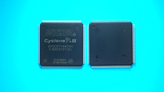
| EP2C5T144C8N COUNTRY OF ORIGIN | ||||||||||||||||||||||||||||||||||||||||||||||||||||||||||||||||||||||||||||||||||||||
| EP2C5T144C8N PARAMETRIC INFO | ||||||||||||||||||||||||||||||||||||||||||||||||||||||||||||||||||||||||||||||||||||||
| EP2C5T144C8N PACKAGE INFO | ||||||||||||||||||||||||||||||||||||||||||||||||||||||||||||||||||||||||||||||||||||||
| EP2C5T144C8N MANUFACTURING INFO | ||||||||||||||||||||||||||||||||||||||||||||||||||||||||||||||||||||||||||||||||||||||
| EP2C5T144C8N PACKAGING INFO | ||||||||||||||||||||||||||||||||||||||||||||||||||||||||||||||||||||||||||||||||||||||
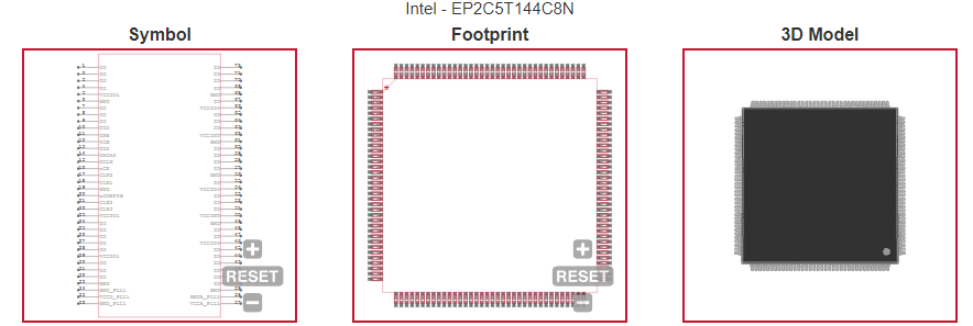
| EP2C5T144C8N ECAD MODELS | ||||||||||||||||||||||||||||||||||||||||||||||||||||||||||||||||||||||||||||||||||||||
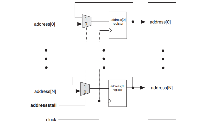
| EP2C5T144C8N FYNCTONAL BLOCK DIAGRAM | ||||||||||||||||||||||||||||||||||||||||||||||||||||||||||||||||||||||||||||||||||||||
| EP2C5T144C8N APPLICATIONS | ||||||||||||||||||||||||||||||||||||||||||||||||||||||||||||||||||||||||||||||||||||||
| |
||||||||||||||||||||||||||||||||||||||||||||||||||||||||||||||||||||||||||||||||||||||
| COUNTRY OF ORIGIN | ||||||||||||||||||||||||||||||||||||||||||||||||||||||||||||||||||||||||||||||||||||||
| Malaysia | ||||||||||||||||||||||||||||||||||||||||||||||||||||||||||||||||||||||||||||||||||||||
| |
||||||||||||||||||||||||||||||||||||||||||||||||||||||||||||||||||||||||||||||||||||||
| PARAMETRIC INFO | ||||||||||||||||||||||||||||||||||||||||||||||||||||||||||||||||||||||||||||||||||||||
|
||||||||||||||||||||||||||||||||||||||||||||||||||||||||||||||||||||||||||||||||||||||
| PACKAGE INFO | ||||||||||||||||||||||||||||||||||||||||||||||||||||||||||||||||||||||||||||||||||||||
|
||||||||||||||||||||||||||||||||||||||||||||||||||||||||||||||||||||||||||||||||||||||
| MANUFACTURING INFO | ||||||||||||||||||||||||||||||||||||||||||||||||||||||||||||||||||||||||||||||||||||||
|
||||||||||||||||||||||||||||||||||||||||||||||||||||||||||||||||||||||||||||||||||||||
| PACKAGING INFO | ||||||||||||||||||||||||||||||||||||||||||||||||||||||||||||||||||||||||||||||||||||||
|
||||||||||||||||||||||||||||||||||||||||||||||||||||||||||||||||||||||||||||||||||||||
| ECAD MODELS | ||||||||||||||||||||||||||||||||||||||||||||||||||||||||||||||||||||||||||||||||||||||
 |
||||||||||||||||||||||||||||||||||||||||||||||||||||||||||||||||||||||||||||||||||||||
| |
||||||||||||||||||||||||||||||||||||||||||||||||||||||||||||||||||||||||||||||||||||||
| FYNCTONAL BLOCK DIAGRAM | ||||||||||||||||||||||||||||||||||||||||||||||||||||||||||||||||||||||||||||||||||||||
 |
||||||||||||||||||||||||||||||||||||||||||||||||||||||||||||||||||||||||||||||||||||||
| APPLICATIONS | ||||||||||||||||||||||||||||||||||||||||||||||||||||||||||||||||||||||||||||||||||||||
| ■ Up to 150 18 × 18 multipliers | ||||||||||||||||||||||||||||||||||||||||||||||||||||||||||||||||||||||||||||||||||||||
| ■ Up to 1.1 Mbit of on-chip embedded memory | ||||||||||||||||||||||||||||||||||||||||||||||||||||||||||||||||||||||||||||||||||||||
| ■ High-speed interfaces to external memory | ||||||||||||||||||||||||||||||||||||||||||||||||||||||||||||||||||||||||||||||||||||||
| ■ DSP intellectual property (IP) cores | ||||||||||||||||||||||||||||||||||||||||||||||||||||||||||||||||||||||||||||||||||||||
| ■ DSP Builder interface to The Mathworks Simulink and Matlab design environment | ||||||||||||||||||||||||||||||||||||||||||||||||||||||||||||||||||||||||||||||||||||||
| ■ DSP Development Kit, Cyclone II Edition | ||||||||||||||||||||||||||||||||||||||||||||||||||||||||||||||||||||||||||||||||||||||
| |