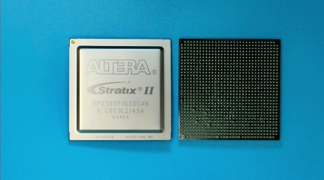
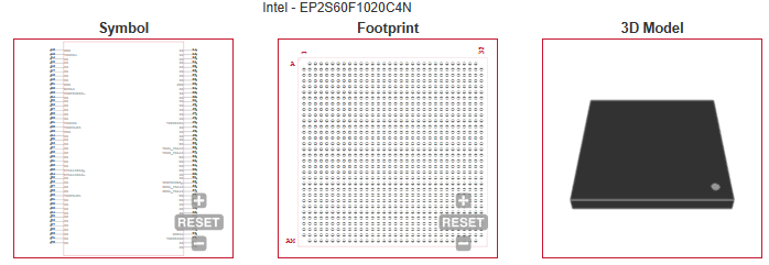
| Device Logic Units |
60440 |
| Device Logic Cells |
60440 |
| Maximum Number of User I/Os |
718 |
| Number of I/O Banks |
8 |
| Device Number of DLLs/PLLs |
12 |
| Number of Multipliers |
144 (18x18) |
| Number of Regional Clocks |
32 |
| Tradename |
Stratix |
| Maximum I/O Performance |
1Gbps |
| RAM Bits (Kbit) |
2484.6 |
| Total Number of Block RAM |
2+255+329 |
| Program Memory Type |
SRAM |
| Series name |
Stratix® II |
| Process Technology |
90nm |
| Speed Grade |
4 |
| Dedicated DSP |
36 |
| Differential I/O Standards Supported |
LVPECL|LVDS |
| Single-Ended I/O Standards Supported |
LVTTL|CMOS|SSTL|HSTL |
| Giga Multiply Accumulates per Second |
37.8 |
| External Memory Interface |
DDR SDRAM|DDR2 SDRAM|RLDRAM II|QDRII+SRAM |
| Mega Multiply Accumulates per second |
37800 |
| Copy Protection |
no |
| Shift Registers |
Utilize Memory |
| Supported IP Core |
Viterbi Compiler, High-Speed Parallel Decoder|RapidIO to AXI Bridge Controller (RAB)|PowerPC/SH/1960 System Controller|32/64-bit PCI-X bus Master/Target interface Core, 66/100/133Mhz |
| Programmability |
no |
| Supported IP Core Manufacture |
Altera/CAST, Inc/Barco Silex/Mobiveil, Inc/Eureka Technology Inc/PLDA |
| In-System Programmability |
yes |
| Reprogrammability Support |
no |
| Maximum Internal Frequency (MHz) |
711.24 |
| Number of Global Clocks |
16 |
| Maximum Operating Supply Voltage (V) |
1.25 |
| I/O Voltage (V) |
1.5|1.8|2.5|3.3 |
| Minimum Operating Temperature (°C) |
0 |
| Maximum Operating Temperature (°C) |
85 |
| Temperature Flag |
June |
| Supplier Temperature Rating |
Commercial |
| Digital Control Impedance |
no |
| Minimum Operating Supply Voltage (V) |
1.15 |
| Typical Operating Supply Voltage (V) |
1.2 |
| Tolerant Configuration Interface Voltage (V) |
1.5|1.8|2.5|3.3 |
| Maximum Storage Temperature (°C) |
150 |
| Minimum Storage Temperature (°C) |
-65 |

