 |
||||||||||||||||||||||||||||||||||||||||||||||||||||||||||||||||||||||||||||
| Cyclone III device family offers the following features: |
||||||||||||||||||||||||||||||||||||||||||||||||||||||||||||||||||||||||||||
| ■ Lowest power consumption with TSMC low-power process technology andAltera® power-aware design flow |
||||||||||||||||||||||||||||||||||||||||||||||||||||||||||||||||||||||||||||
| ■ Low-power operation offers the following benefits: ■ Extended battery life for portable and handheld applications ■ Reduced or eliminated cooling system costs ■ Operation in thermally-challenged environments |
||||||||||||||||||||||||||||||||||||||||||||||||||||||||||||||||||||||||||||
| ■ Hot-socketing operation support |
||||||||||||||||||||||||||||||||||||||||||||||||||||||||||||||||||||||||||||
| Cyclone III LS devices offer the following design security features: |
||||||||||||||||||||||||||||||||||||||||||||||||||||||||||||||||||||||||||||
| ■ Configuration security using advanced encryption standard (AES) with 256-bitvolatile key |
||||||||||||||||||||||||||||||||||||||||||||||||||||||||||||||||||||||||||||
| ■ Routing architecture optimized for design separation flow with the Quartus® IIsoftware ■ Design separation flow achieves both physical and functional isolationbetween design partitions |
||||||||||||||||||||||||||||||||||||||||||||||||||||||||||||||||||||||||||||
| ■ Ability to disable external JTAG port |
||||||||||||||||||||||||||||||||||||||||||||||||||||||||||||||||||||||||||||
| ■ Error Detection (ED) Cycle Indicator to core ■ Provides a pass or fail indicator at every ED cycle ■ Provides visibility over intentional or unintentional change of configurationrandom access memory (CRAM) bits |
||||||||||||||||||||||||||||||||||||||||||||||||||||||||||||||||||||||||||||
| ■ Ability to perform zeroization to clear contents of the FPGA logic, CRAM,embedded memory, and AES key |
||||||||||||||||||||||||||||||||||||||||||||||||||||||||||||||||||||||||||||
| ■ Internal oscillator enables system monitor and health check capabilities |
||||||||||||||||||||||||||||||||||||||||||||||||||||||||||||||||||||||||||||
| ■ High memory-to-logic and multiplier-to-logic ratio |
||||||||||||||||||||||||||||||||||||||||||||||||||||||||||||||||||||||||||||
| ■ High I/O count, low-and mid-range density devices for user I/O constrainedapplications ■ Adjustable I/O slew rates to improve signal integrity ■ Supports I/O standards such as LVTTL, LVCMOS, SSTL, HSTL, PCI, PCI-X,LVPECL, bus LVDS (BLVDS), LVDS, mini-LVDS, RSDS, and PPDS ■ Supports the multi-value on-chip termination (OCT) calibration feature toeliminate variations over process, voltage, and temperature (PVT) |
||||||||||||||||||||||||||||||||||||||||||||||||||||||||||||||||||||||||||||
| ■ Four phase-locked loops (PLLs) per device provide robust clock management andsynthesis for device clock management, external system clock management, andI/O interfaces ■ Five outputs per PLL ■ Cascadable to save I/Os, ease PCB routing, and reduce jitter ■ Dynamically reconfigurable to change phase shift, frequency multiplication ordivision, or both, and input frequency in the system without reconfiguring thedevice |
||||||||||||||||||||||||||||||||||||||||||||||||||||||||||||||||||||||||||||
| ■ Remote system upgrade without the aid of an external controller |
||||||||||||||||||||||||||||||||||||||||||||||||||||||||||||||||||||||||||||
| ■ Dedicated cyclical redundancy code checker circuitry to detect single-event upset(SEU) issues |
||||||||||||||||||||||||||||||||||||||||||||||||||||||||||||||||||||||||||||
| ■ Nios® II embedded processor for Cyclone III device family, offering low cost andcustom-fit embedded processing solutions |
||||||||||||||||||||||||||||||||||||||||||||||||||||||||||||||||||||||||||||
| ■ Wide collection of pre-built and verified IP cores from Altera and AlteraMegafunction Partners Program (AMPP) partners |
||||||||||||||||||||||||||||||||||||||||||||||||||||||||||||||||||||||||||||
| ■ Supports high-speed external memory interfaces such as DDR, DDR2,SDR SDRAM, and QDRII SRAM ■ Auto-calibrating PHY feature eases the timing closure process and eliminatesvariations with PVT for DDR, DDR2, and QDRII SRAM interfaces |
||||||||||||||||||||||||||||||||||||||||||||||||||||||||||||||||||||||||||||
| CATALOG | ||||||||||||||||||||||||||||||||||||||||||||||||||||||||||||||||||||||||||||
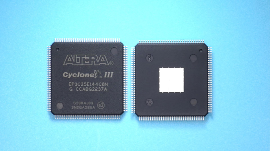
| EP3C25E144C8N COUNTRY OF ORIGIN |
||||||||||||||||||||||||||||||||||||||||||||||||||||||||||||||||||||||||||||
| EP3C25E144C8N PARAMETRIC INFO |
||||||||||||||||||||||||||||||||||||||||||||||||||||||||||||||||||||||||||||
| EP3C25E144C8N PACKAGE INFO |
||||||||||||||||||||||||||||||||||||||||||||||||||||||||||||||||||||||||||||
| EP3C25E144C8N MANUFACTURING INFO |
||||||||||||||||||||||||||||||||||||||||||||||||||||||||||||||||||||||||||||
| EP3C25E144C8N PACKAGING INFO |
||||||||||||||||||||||||||||||||||||||||||||||||||||||||||||||||||||||||||||
| COUNTRY OF ORIGIN |
||||||||||||||||||||||||||||||||||||||||||||||||||||||||||||||||||||||||||||
| Philippines |
||||||||||||||||||||||||||||||||||||||||||||||||||||||||||||||||||||||||||||
| Malaysia |
||||||||||||||||||||||||||||||||||||||||||||||||||||||||||||||||||||||||||||
| PARAMETRIC INFO |
||||||||||||||||||||||||||||||||||||||||||||||||||||||||||||||||||||||||||||
|
||||||||||||||||||||||||||||||||||||||||||||||||||||||||||||||||||||||||||||
| PACKAGE INFO |
||||||||||||||||||||||||||||||||||||||||||||||||||||||||||||||||||||||||||||
|
||||||||||||||||||||||||||||||||||||||||||||||||||||||||||||||||||||||||||||
| MANUFACTURING INFO |
||||||||||||||||||||||||||||||||||||||||||||||||||||||||||||||||||||||||||||
|
||||||||||||||||||||||||||||||||||||||||||||||||||||||||||||||||||||||||||||
| PACKAGING INFO |
||||||||||||||||||||||||||||||||||||||||||||||||||||||||||||||||||||||||||||
|
||||||||||||||||||||||||||||||||||||||||||||||||||||||||||||||||||||||||||||