| Channel Type |
N |
| Channel Mode |
Enhancement |
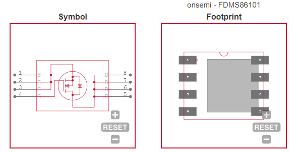
| Configuration |
Single Quad Drain Triple Source |
| Maximum Drain Source Voltage (V) |
100 |
| Material |
Si |
| Maximum Continuous Drain Current (A) |
12.4 |
| Maximum Gate Source Voltage (V) |
±20 |
| Maximum Drain Source Resistance (mOhm) |
8@10V |
| Typical Gate Charge @ Vgs (nC) |
39@10V|22@5V |
| Typical Gate Charge @ 10V (nC) |
39 |
| Maximum Power Dissipation (mW) |
2500 |
| Process Technology |
TMOS |
| Category |
Power MOSFET |
| Typical Output Capacitance (pF) |
460 |
| Typical Input Capacitance @ Vds (pF) |
2255@50V |
| Typical Turn-On Delay Time (ns) |
15 |
| Typical Turn-Off Delay Time (ns) |
27 |
| Typical Fall Time (ns) |
7 |
| Typical Rise Time (ns) |
11 |
| Number of Elements per Chip |
1 |
| Minimum Storage Temperature (°C) |
-55 |
| Maximum Storage Temperature (°C) |
150 |
| Minimum Operating Temperature (°C) |
-55 |
| Maximum Operating Temperature (°C) |
150 |