 |
|
| • Optimized for Complementary Driven Half-Bridge Soft-Switching Converters |
| • Can be Applied to Various Topologies:Asymmetric PWM Half-Bridge Converters, AsymmetricPWM Flyback Converters,Asymmetric PWM Forward Converters,Active Clamp Flyback Converters |
| • High Efficiency through Zero-Voltage-Switching (ZVS) |
| • Internal SuperFET TMs with Fast-Recovery Type Body Diode (tn=120 ns) |
| • Fixed Dead Time (200 ns) Optimized for MOSFETs |
| • Up to 300 kHz Operating Frequency |
| • Internal Soft-Start |
| • Pulse-by-Pulse Current Limit |
| • Burst-Mode Operation for Low Standby Power Consumption |
• Protection Functions:Over-Voltage Protection(OVP), Over-Load Protection (OLP),Abnormal Over- Current Protection (AOCP),Internal ThermalShutdown(TSD)
|
|
| CATALOG |
| FSFA2100 COUNTRY OF ORIGIN |
| FSFA2100 LIFECYCLE |
| FSFA2100 PARAMETRIC INFO |
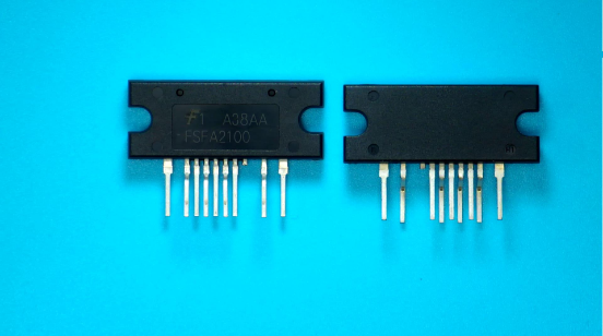
| FSFA2100 PACKAGE INFO |
| FSFA2100 MANUFACTURING INFO |
| FSFA2100 PACKAGING INFO |
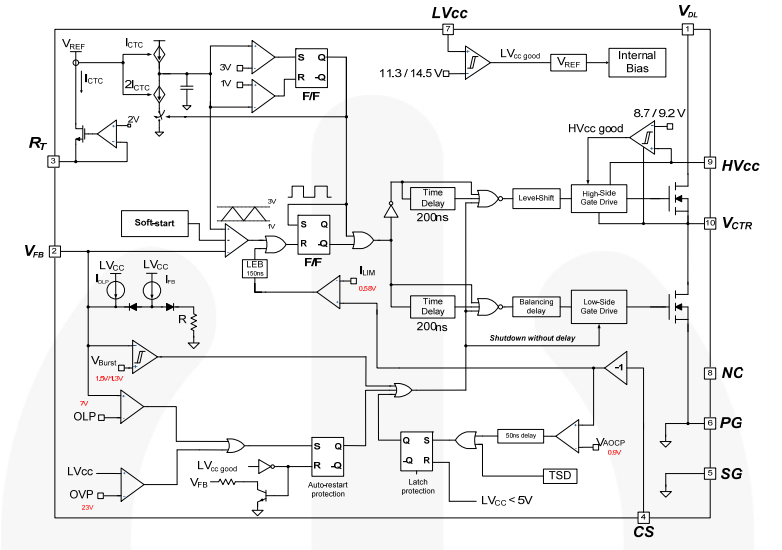
| FSFA2100 FUNCTONAL BLOCK DIAGRAM |
| FSFA2100 APPLICATIONS |
|
| COUNTRY OF ORIGIN |
| China |
|
| LIFECYCLE |
Obsolete
Jun 23,2022 |
| |
| PARAMETRIC INFO |
| Topology |
Flyback |
| Soft Start Optio |
Yes |
| Switching Frequency (kHz) |
106 |
| Minimum Under Voltage Lock Out (V) |
13 |
| Typical Under Voltage Lock Out (V) |
14.5 |
| Maximum Under Voltage Lock Out (V) |
16 |
| Minimum Supply Voltage (V) |
-0.3 |
| Maximum Supply Voltage (V) |
25 |
| Maximum Operating Current (mA) |
11 |
| Minimum Operating Temperature (°C) |
-40 |
| Maximum Operating Temperature (°C) |
130 |
| Minimum Storage Temperature (°C) |
-55 |
| Maximum Storage Temperature (°C) |
150 |
|
| PACKAGE INFO |
| Supplier Package |
SIP |
| Basic Package Type |
Through Hole |
| Pin Count |
9 |
| Lead Shape |
Through Hole |
| PCB |
9 |
| Tab |
N/R |
| Pin Pitch (mm) |
1.27 |
| Package Length (mm) |
26.2(Max) |
| Package Width (mm) |
3.4(Max) |
| Package Height (mm) |
10.7(Max) |
| Package Diameter (mm) |
N/R |
| Seated Plane Height (mm) |
14.5(Max) |
| Mounting |
Through Hole |
| Package Weight (g) |
N/A |
| Package Material |
Plastic |
| Package Description |
Single In Line Package |
| Package Family Name |
SIP |
| Jedec |
N/A |
|
| MANUFACTURING INFO |
| MSL |
N/R |
| Maximum Reflow Temperature (°C) |
N/R |
| Reflow Solder Time (Sec) |
N/R |
| Maximum Wave Temperature (°C) |
260 |
| Wave Solder Time (Sec) |
10 |
| Wave Temp. Source |
Link to Datasheet |
| Lead Finish(Plating) |
Matte Sn annealed |
| Under Plating Material |
N/A |
| Terminal Base Material |
CuFeZnP |
|
| PACKAGING INFO |
| Packaging |
Tube |
| Quantity Of Packaging |
475 |
|
| FUNCTONAL BLOCK DIAGRAM |
 |
|
| APPLICATIONS |
| • PDP and LCD TVs . |
| • Desktop PCs and Servers |
| • Adapters |
| • Telecom Power Supplies |
|