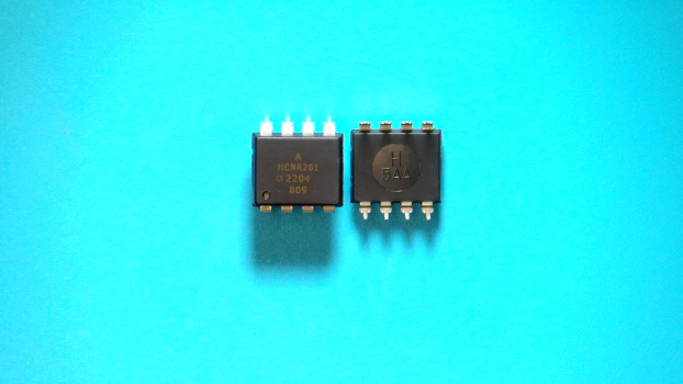
|
|
• Low nonlinearity: 0.01%
|
• K3 (IPD2/IPD1) transfer gain
HCNR200: ±15%
HCNR201: ±5%
|
• Low gain temperature coefficient: 65 ppm/°C
|
| • Wide bandwidth – DC to >1 MHz
|
| • Worldwide safety approval
– UL 1577 recognized (5 kV rms/1 min. rating)
– CSA approved
– IEC/EN/DIN EN 60747-5-5 approved
VIORM = 1414 Vpeak (option -050E/-350E/-550E) |
| • Surface mount option available (Option #300) |
| • 8-pin DIP package – 0.400-in. spacing
|
| • Allows flexible circuit design
|
|
| CATALOG |
| HCNR201-000E COUNTRY OF ORIGIN |
HCNR201-000E PARAMETRIC INFO
|
HCNR201-000E PACKAGE INFO
|
HCNR201-000E MANUFACTURING INFO
|
| HCNR201-000E APPLICATIONS |
|
| COUNTRY OF ORIGIN |
| Malaysia |
|
PARAMETRIC INFO
|
| Input Type |
DC |
| Maximum Working Insulation Voltage (V) |
1414 |
| Typical Bandwidth (MHz) |
9 |
| Output Type |
DC |
| Output Device |
Linear Photovoltaic |
| standard |
CSA|UL |
| Number of Channels per Chip |
1 |
| Minimum Forward Voltage (V) |
1.2 |
| Typical Forward Voltage (V) |
1.6 |
| Maximum Forward Voltage (V) |
1.95 |
| Maximum Forward Current (mA) |
25 |
| Maximum Reverse Voltage (V) |
2.5 |
| Minimum Isolation Voltage (Vrms) |
5000 |
| Maximum Power Dissipation (mW) |
60 |
| Minimum Operating Temperature (°C) |
-40 |
| Maximum Operating Temperature (°C) |
85 |
| Maximum Data Rate |
1.5MHz(Typ) |
| Maximum Storage Temperature (°C) |
85 |
| Minimum Storage Temperature (°C) |
-40 |
|
|
PACKAGE INFO
|
| Supplier packaging |
PDIP W |
| Basic package type |
Through Hole |
| Number of pins |
8 |
| Pin shape |
Through Hole |
| PCB |
8 |
| ears |
N/R |
| Package length (mm) |
11.3 |
| Package width (mm) |
9 |
| Package height (mm) |
5.1(Max)-0.51(Min) |
| Package diameter (mm) |
N/R |
| Install |
Through Hole |
| Packaging materials |
Plastic |
| package instruction |
Plastic Dual In Line Package Wide Body |
| Package series name |
DIP |
|
|
MANUFACTURING INFO
|
| MSL |
1 |
| Maximum reflow temperature (°C) |
245 |
| Reflow soldering time (seconds) |
15 |
| Reflow temperature source |
Link to datasheet |
| Maximum wave soldering temperature (°C) |
260 |
| Wave soldering time (seconds) |
10 |
| Wave soldering temperature source |
Link to datasheet |
| Lead Finish(Plating) |
Matte Sn annealed |
| Plating materials |
not applicable |
| Terminal Base Material |
Alloy 42 |
|
|
APPLICATIONS
|
• Low cost analog isolation
|
• Telecom: Modem, PBX
|
• Industrial process control:
Transducer isolator
Isolator for thermocouples 4 mA to 20 mA loop isolation
|
| • SMPS feedback loop, SMPS feedforward |
| • Monitor motor supply voltage |
| • Medical |
| |
